Jawed
Legend
Jaws said:Well, the 'leak' mentions that each of the 48 ALUs has a 'vector' and 'scalar' unit. So that's 48 vector and 48 scalar units. I expect the vector unit to be 4-way SIMD (128 bit, 4* 32 bit) and both units to be 32bit single precision capable. Also capable of Floats and Integers.
Different peeps, as I'm learning the hard way, have different ways of counting ALUs. ATI counts 76 non-texturing ALUs in the vertex and pixel shaders of X800.
Reviewers seem to count them as 16 pipelines x2 + 6 pipelines x2 = 44 ALUs.
:?
What's on my mind, apart from anything else, is the transistor budget for the ALUs.
If you assume that the transistors required per dimension and per bit of each ALU, then you get this rather interesting result:
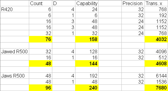
(I've edited the picture to show the vector and scalar parts of Jaws's proposal separately)
And that's before you add in SM3 functionality into the ALUs.
Jawed
