AMD: Speculation, Rumors, and Discussion (Archive)

Status
Not open for further replies.
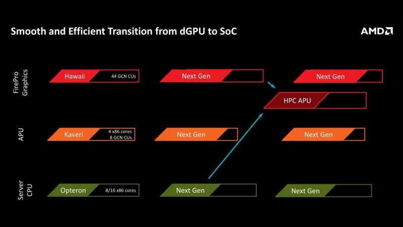
AMD has presented a GPU roadmap up to 2020 at the PC Cluster Consortium (from news.mynavi.jp).

005l.jpg


news.mynavi.jp said:
In the graphics field, in 2012 "Tahiti", it has been developed a "Hawaii" in 2014, new graphics chips every two years: go to develop (dGPU discrete GPU). And, I will continue the cycle of incorporating it into the APU to the next odd-numbered years. As a result, APU of 2019 is that will have the computing performance of a few TFlops.
According to WCCFTech, the two-year cycle is specifically regarding APUs, and discrete GPUs will be updated more frequently.

original.jpg


The HPC APU scheduled for 2017 may have a TDP of up to 200-300 W.

Is it too much to hope for a consumer variant of that APU?
 
One oddity is that FirePro encompasses an APU and what used to be called FireStream.
It still seems to me that some level of CPU integration would be helpful for that line, so would this be considered a split?

APUs tend to take a bit longer to catch up on the GPU side, and until AMD's CPU advancement cratered the same was true there. Would the APU that comes after the HPC APU be the stripped-down consumer variant?

In that scenario, the HPC APU could be a pathfinder for the lines above and below it in the chart.
 
>Is it too much to hope for a consumer variant of that APU?

Hope so!
Now that Intel isn't implementing OpenCL double precision for their IGPs (despite having the hardware...)
 
The HPC APU scheduled for 2017 may have a TDP of up to 200-300 W.

Is it too much to hope for a consumer variant of that APU?
If there is really one, logically speaking AMD would sell it to wherever makes sense in profits. In other words, I don't see why AMD wouldn't sell consumer variants to amortize the cost with a larger base.
 
AMD prepping Greenland Graphics for 2016

"Details are limited, apart of the fact that Greenland can end up in the next generation APU such as K12, making the architecture quite scalable. High Bandwidth Memory combined with new K12 cores might create the fastest integrated product of all time, and let's not forget that AMD is putting a lot of emphasis on Heterogeneous System Architecture (HSA) and the compute side of things. With the help of HBM-powered Greenland that can end up with 500GB/s bandwidth, along with multiple Zen 64-bit CPU cores, you can expect quite a lot of compute performance from this new integrated chip."

The rumor originates from Fudzilla which mentioned that the Radeon R400 series will be called the “Arctic Islands” family. They do not mentioned which graphics cards or branding the Greenland GPUs will use. It is also mentioned that AMD will be launching Fiji GPU in late June or Q2 2015. Greenland could end up in the K12 ARM and x86 Zen core architecture (servers) which are due in 2016 as well.

http://www.guru3d.com/news-story/amd-prepping-greenland-gpu-for-2016.html
 
I'd say 3DCenter is being purely speculative.
They just take die area for 28 nm GCN 1.0 HD7000 series chips (incorrectly naming them "Northern Islands", which was HD6000 series "Terascale2") and try to scale their specs to 14 nm - however they don't seem to understand that process shrink from 28 nm down to 14 nm will quadruple the transistor count on the same die area, not just double it.
So, meh.
 
The foundries are not scaling their interconnect pitch in the 20nm to 16/14nm transition, so the density gains are incremental over the transition to 20.
 
I'd say 3DCenter is being purely speculative.
They just take die area for 28 nm GCN 1.0 HD7000 series chips (incorrectly naming them "Northern Islands", which was HD6000 series "Terascale2") and try to scale their specs to 14 nm - however they don't seem to understand that process shrink from 28 nm down to 14 nm will quadruple the transistor count on the same die area, not just double it.
So, meh.

It isn't really quadruple, density doesn't go up that much even though you'd think it would given the name. Mostly because the name is disconnected from most engineering reality and has slowly gotten so over time, so the name is really just for marketing purposes.

Regardless I would agree it's useless speculation. "Whatever density/feature size you call it" Finfet is certainly going to be featured in a new series of GPUs from both AMD and Nvidia, probably early next year. Samsung, TSMC, and Global Foundries will all have scaled up their capacity of such by then, and gotten rid of enough manufacturing defects, to make huge chips like GPUs possible. But considering AMD has made at least a handful of changes each "generation" (Call it GCN 1.0, 1.1, 1.2, whatever) it's doubtful they'd just let that trend drop next year for no reason. Especially as the "numbers" there are as vague as possible. Especially as AMD's measurements are in its own "stream processors".
 
The foundries are not scaling their interconnect pitch in the 20nm to 16/14nm transition, so the density gains are incremental over the transition to 20.

Yeah, I think they're claiming something like a 15% increase in density over 20nm. I guess in practice it will be more for some types of structures, and less for others.
 
What would AMD possibly gain from adopting nvidia's naming scheme? Also there is no way a 500+mm^2 gpu would be possible on 14nm by next year.
 
Why not? [Citation needed]... ;)
My best guess is that he is referring to Dark Silicon?
Wikipedia:
Dark silicon is a term used in the electronics industry. In the nano-era, transistor scaling and voltage scaling are no longer in line with each other, resulting in the failure of Dennard scaling. This discontinuation of Dennard scaling has led to sharp increases in power densities that hamper powering-on all the transistors simultaneously at the nominal voltage, while keeping the chip temperature in the safe operating range. "Dark Silicon" refers to the amount of silicon that cannot be powered-on at the nominal operating voltage for a given thermal design power (TDP) constraint. According to recent studies, researchers from different groups have projected that, at 8 nm technology nodes, the amount of Dark Silicon may reach up to 50%-80%[1] depending upon the processor architecture, cooling technology, and application workloads. Dark Silicon may be unavoidable even in server workloads with abundance of inherent client request-level parallelism.[2]
 
What triggers me the most in those rumours is the obvious use of nVidia's nomenclature for performance targets.
AI100, AI104, AI106 and AI107? Really?

I would swallow if it was AI-100, then AI-V170, then AI-V140 and AI-V130 :p
 
Dark Silicon doesn't limit the production of a large die.

He probably indicating that 14nm won't be mature enough to handle 500mm2 chips in 2016
 
It isn't really quadruple, density doesn't go up that much even though you'd think it would given the name.
I think they're claiming something like a 15% increase in density over 20nm. I guess in practice it will be more for some types of structures, and less for others.
Hell yeah, I thought the whole point of ITRS roadmap is that each new process node is exactly SQRT(2)/2 =0.707 of the previous node, which results either 2x the number of transistors on the same die area, or 1/2 die area for the same number of transistors...

But even if 29% downscaling does not materialize, ~20% on each node transition still amounts to almost tripling the transistor count on the same die area, or the same number of transistors on 1/3rd of the die area.

considering AMD has made at least a handful of changes each "generation" (Call it GCN 1.0, 1.1, 1.2, whatever) it's doubtful they'd just let that trend drop next year for no reason.
These are mostly microcode changes which do not amount to a great increase of transistor budget.

In massively multithreaded cores, you don't really need complex superscalar processors that require large execution blocks. You'd rather have several thousand basic processors, just like in GCN.

So I'd expect they'd rather spend additional transistor budget on bigger/wider caches/TLBs to support more virtual memory for Volume Tiled Resources and new rasterizer features like Conservative Rasterization and Rasterizer Ordered Views, rather than completely revise the shader processor architecture once again. Or maybe use the finer process node to reduce the die area and improve defect rate for better economies of scale.
 
What would AMD possibly gain from adopting nvidia's naming scheme?
What triggers me the most in those rumours is the obvious use of nVidia's nomenclature for performance targets.
AI100, AI104, AI106 and AI107? Really?
If you read Google translation, they say the exact code names are unknown, so chip nomenclature is completely made-up - and being hard-core Nvidia fanboys, they probably just couldn't resist using Nvidia-like names :p
 
Hell yeah, I thought the whole point of ITRS roadmap is that each new process node is exactly SQRT(2)/2 =0.707 of the previous node, which results either 2x the number of transistors on the same die area, or 1/2 die area for the same number of transistors...
ITRS tries to produce a projection of what is coming, based on the accumulated opinion of experts in the field.
It doesn't have much to do with what marketing puts on the brochures for the manufacturers.
 
Why not? [Citation needed]... ;)
I don't really have a source but I don't expect 14nm to ramp faster than 28nm did and the time between the first 28nm part (Tahiti) and the first really large chip (GK110) was about a year later. 14nm GPUs will likely launch mid 2016 and a refresh line up with a larger die flag ship can launch in 2017. It makes too much sense given how it worked out like this for 28nm and it will probably be a long time until 10nm node comes online.
 
Status
Not open for further replies.
Back
Top