Yep, twice. But that don't speak well for the SP rate, if this assertion is correct.
Seems fine to me compared to nVidia's offering. From the same article, Kepler will be somewhere around 2TF for SP.
Follow along with the video below to see how to install our site as a web app on your home screen.
Note: This feature may not be available in some browsers.
Yep, twice. But that don't speak well for the SP rate, if this assertion is correct.
My interpretation of that is more like 2.5TF, possibly even 3TF, depending on the power definition nvidia uses there for the 5gflop/w DP figure (we all know GTX 580 uses more power than the TDP figure at full load). 2TF would be hardly faster than GTX580 (well as far as peak flop rate is concerned at least), only 25% more. I'd definitely expect more.Seems fine to me compared to nVidia's offering. From the same article, Kepler will be somewhere around 2TF for SP.
My interpretation of that is more like 2.5TF, possibly even 3TF, depending on the power definition nvidia uses there for the 5gflop/w DP figure (we all know GTX 580 uses more power than the TDP figure at full load). 2TF would be hardly faster than GTX580 (well as far as peak flop rate is concerned at least), only 25% more. I'd definitely expect more.
Is there any reason to suspect that a ~32 CU version of GCN would have a significantly lower clock speed than 850 MHz?In any case 2TF is a pretty lowball estimate for GCN. 32 CU's at 850Mhz would pull ~3.5TF.
Thanks. That's the only reason I could think of that would give ~2TFlops of SP but it would be such a huge step backwards, according to my minimal understanding.Well each SIMD lane can do one SP FMA per cycle, so that's 2 FLOP/cycle, yes.
Thanks. That's the only reason I could think of that would give ~2TFlops of SP but it would be such a huge step backwards, according to my minimal understanding.
All the technical details aside, do we expect them to stick with a 256 bit bus? Presumably they'll be able to up the GDDR5 speed to 6 ghz (from what i gather, it cant be pushed much further?). But this is hardly a 10% increase in b/w from Cayman. If their aim is to double performance over Cayman, im guessing they will be b/w constrained. So whats on the cards? 384 bit? Not sure they'd need or whether they'd be even willing to try 512 bit after their experience with R600.
Which, additionally, would be a pretty good match for a linear projection of recent GPU capabilities from X1000 series onwards.In any case 2TF is a pretty lowball estimate for GCN. 32 CU's at 850Mhz would pull ~3.5TF.
Yeah, I didn't make any sense did I? My thoughts and typing didn't line up very well.
That's exactly what current ALUs can do, why would that be a step backwards?
I'd not be surprised if the fastest chip would have a lower frequency, though I wouldn't expect that much lower (maybe 750-800Mhz). At least the current designs require too much voltage to be able to run at the 850-900Mhz frequencies with good power efficiency compared to the lower clocked parts. And power draw (and hence also thermal) problems certainly won't get any better.Is there any reason to suspect that a ~32 CU version of GCN would have a significantly lower clock speed than 850 MHz?
Well, Cypress/5870 wasn't that bad in that regard.I'd not be surprised if the fastest chip would have a lower frequency, though I wouldn't expect that much lower (maybe 750-800Mhz). At least the current designs require too much voltage to be able to run at the 850-900Mhz frequencies with good power efficiency compared to the lower clocked parts. And power draw (and hence also thermal) problems certainly won't get any better.
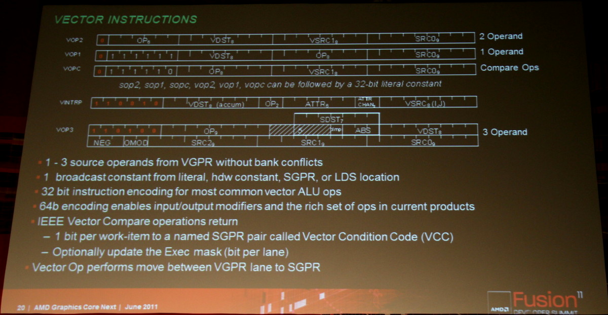
an awful lot of comparison instructions(?!?)
Hmm lots of cmps indeed. Anyone know what they do? I mean there's a full set of them for each operator (ne, lt and so on) on all datatypes (f32, f64, u32, u64, i32, i64) but what's the cmp/cmpx/cmps/cmpsx doing (though the "s" versions are only for floats - maybe versions ignoring/not ignoring sign)?
Coming back to the compares. Rpg.314 gave already a possible explanation for the comps instructions. I just stumbled across one for the cmpx and cmpsx. Just look at the description of the instruction format:Compare element wise with scalar?
")
You also have to consider though that the lower-end versions are probably using worse chips, where basically all chips have to qualify.Well, Cypress/5870 wasn't that bad in that regard.
Oh, I'm not suggesting the power envelope wouldn't be similar to HD6970 even with reduced clocks...There are enough "all I care about is raw performance, noise and power matter not"-enthusiasts out there though, so I wouldn't be surprised to see at least one SKU at a power envelope similar to 6970.
What is going on with Southern Islands, the next generation ATI (NYSE:AMD) graphics card? When is it coming out? What is it? The last one, what is it, is easy. AMD told us all about it at Fusion 11, or at least the shader architecture, so the only open questions are how many of them, and when will we see it? Both are dictated by TSMC’s 28nm process, or are they?
OffiCIal word is that TSMC is coming out with 28nm products in Q3 of this year, that would be some time from next week to the end of September. Given the foundry’s track record on 40nm, we are fairly skeptical about this. Moles say that 28nm non-HKMG is doing just peachy, but the 28nm HKMG process is having the proverbial issues. Lets hope these are the normal bring up/teething issues and things are on time for the sake of the entire industry.
Back to Southern Islands (SI). At Computex, AMD was telling all the vendors Q1, which means TSMC would start ramping in Q4, and have volume in Q1, but in reality, don’t count on things going well. The problem is that other sources are now saying that things are going really really well, and signs are looking like it is September-ish, not February-ish.
If you look at when SI taped out, chips could possibly be on the market in mid-Q3. That date assumes that TSMC is willing, able, and has wafer starts to spare. SemiAccurate is pretty sure that the first is true, the third looks somewhat questionable, and the second is the open question. Considering that there are Apple chips coming off the line now, quite possibly 28nm Apple chips, then that means that TSMC is able, but puts wafer availability in serious doubt.
One other slim but intriguing possibility surrounds SI, is it on 40nm? Northern Islands was originally set for the canceled 32nm process, and was then backported to 40nm, so things like this can and do happen. Could there be some 40nm SIs that come early, then a quick 28nm refresh when our Taiwanese buddies have their wafers ready? Could the line be split between 28 and 40?
Overall, we doubt there will be any 40nm SIs, but technically speaking, it could happen. Southern Islands is much more likely 28nm, and quite possibly coming in very short order. Q3 should be easy if 28nm HKMG works, is on time, and AMD can get the capaCIty it needs. Some other data points show that AMD is looking hard at late August as the earliest possible launch date, but September is more traditional, whatever the process geometry.S|A
Just looked at a Cat11.7 preview driver and things get a bit clearer there.Hmm lots of cmps indeed. Anyone know what they do? I mean there's a full set of them for each operator (ne, lt and so on) on all datatypes (f32, f64, u32, u64, i32, i64) but what's the cmp/cmpx/cmps/cmpsx doing (though the "s" versions are only for floats - maybe versions ignoring/not ignoring sign)? Also some of the operators are a little odd (o? tru?).
; -------- Disassembly --------------------
shader main
  asic(TAHITI)
  type(PS)
                                                            // s_ps_state in s0

  s_mov_b64     s[0:1], exec                                // 00000000: BE80047E
  s_mov_b64     s[2:3], exec                                // 00000004: BE82047E
  v_mov_b32     v0, 0x00010000                              // 00000008: 7E0002FF 00010000
label_0004:
  s_waitcnt     0x0000                                      // 00000010: BF8C0000
  v_cmp_eq_u32  s[4:5], v0, 0                               // 00000014: D1840004 00010100
  s_mov_b64     s[6:7], exec                                // 0000001C: BE86047E
  s_and_b64     exec, s[6:7], s[4:5]                        // 00000020: 87FE0406
  s_andn2_b64   s[2:3], s[2:3], exec                        // 00000024: 8A827E02
  s_cbranch_scc0  label_000F                                // 00000028: BF840004
  s_mov_b64     exec, s[6:7]                                // 0000002C: BEFE0406
  s_and_b64     exec, exec, s[2:3]                          // 00000030: 87FE027E
  v_add_i32     v0, vcc, -1, v0                             // 00000034: 4A0000C1
  s_branch      label_0004                                  // 00000038: BF82FFF5
label_000F:
  s_mov_b64     exec, s[0:1]                                // 0000003C: BEFE0400
  v_mov_b32     v0, 0                                       // 00000040: 7E000280
  v_mov_b32     v1, 0                                       // 00000044: 7E020280
  v_mov_b32     v2, 0                                       // 00000048: 7E040280
  v_mov_b32     v3, 0                                       // 0000004C: 7E060280
  v_nop                                                     // 00000050: 7E000000
  v_nop                                                     // 00000054: 7E000000
  exp           null, off, off, off, off done vm            // 00000058: F8001890 00000000
  s_waitcnt     0x0000                                      // 00000060: BF8C0000
  s_endpgm                                                  // 00000064: BF810000
end; -------- Disassembly --------------------
00 TEX: ADDR(160) CNT(1) VALID_PIX
0 SAMPLE R5, R0.xy0x, t1, s0 UNNORM(XYZW)
01 ALU: ADDR(32) CNT(20) KCACHE0(CB0:0-15)
1 y: F_TO_I ____, R0.y
z: F_TO_I ____, R0.x
w: MOV R3.w, 0.0f
2 z: ADD_INT ____, PV1.z, KC0[0].x
w: LSHL ____, PV1.y, 12
3 x: ADD_INT R6.x, PV2.w, PV2.z
y: XOR_INT R2.y, PV2.w, PV2.w
z: XOR_INT R1.z, PV2.w, PV2.w
w: XOR_INT R2.w, PV2.w, PV2.w
4 x: ADDC_UINT ____, KC0[1].x, PV3.x
y: ADD_INT R3.y, KC0[1].x, PV3.x
z: MOV R0.z, (0x00000001, 1.401298464e-45f).x
5 x: XOR_INT R7.x, PV4.y, PV4.y
y: ADDC_UINT ____, KC0[1].y, PV4.x
w: ADD_INT R4.w, KC0[1].y, PV4.x
6 x: ADDC_UINT ____, KC0[1].z, PV5.y
y: ADD_INT R4.y, KC0[1].z, PV5.y
7 z: ADD_INT R4.z, KC0[1].w, PV6.x
02 LOOP_DX10 i0 FAIL_JUMP_ADDR(8) VALID_PIX
03 ALU: ADDR(52) CNT(1)
8 x: PREDNE_INT ____, R0.z, 0.0f UPDATE_EXEC_MASK BREAK UPDATE_PRED
04 ALU: ADDR(53) CNT(6)
9 x: AND_INT R3.x, R3.y, 0x000003FF
y: BFE_UINT R3.y, R3.y, 0x0000000A, 0x0000000A
z: BIT_ALIGN_INT R0.z, R4.w, R3.y, 0x00000014
w: BIT_ALIGN_INT R1.w, R4.y, R4.w, 0x00000014 VEC_201
05 TEX: ADDR(162) CNT(1) VALID_PIX
10 LD R3.xyz_, R3.xy0w, t0, s0 UNNORM(XYZW)
06 ALU: ADDR(59) CNT(83)
11 x: MULLO_UINT R0.x, R0.z, R3.x
y: MULLO_UINT ____, R0.z, R3.x
z: MULLO_UINT ____, R0.z, R3.x
w: MULLO_UINT ____, R0.z, R3.x
12 x: BIT_ALIGN_INT R2.x, R4.z, R4.y, 0x00000014
y: BIT_ALIGN_INT R1.y, R1.z, R4.z, 0x00000014 VEC_120
z: BIT_ALIGN_INT R1.z, R2.w, R1.z, 0x00000014
w: ADDC_UINT R0.w, PV11.x, R3.y VEC_021
13 x: MULHI_UINT ____, R0.z, R3.x
y: MULHI_UINT ____, R0.z, R3.x
z: MULHI_UINT ____, R0.z, R3.x
w: MULHI_UINT ____, R0.z, R3.x
14 x: SETGT_UINT R4.x, 16777216, 0.0f
y: ADD_INT R0.y, PV13.y, R0.w
z: LSHR R2.z, R2.w, 20
15 x: MULLO_UINT R1.x, R1.w, R3.x
y: MULLO_UINT ____, R1.w, R3.x
z: MULLO_UINT ____, R1.w, R3.x
w: MULLO_UINT ____, R1.w, R3.x
16 x: MULHI_UINT ____, R1.w, R3.x
y: MULHI_UINT ____, R1.w, R3.x
z: MULHI_UINT ____, R1.w, R3.x
w: MULHI_UINT R1.w, R1.w, R3.x
17 y: ADD_INT R3.y, R3.y, R0.x
z: ADDC_UINT ____, R1.x, R0.y
w: ADD_INT R4.w, R0.y, R1.x VEC_120
18 y: ADD_INT R2.y, R2.y, R3.z
z: ADD_INT R0.z, R1.w, PV17.z
w: SETGT_UINT R1.w, PV17.y, 1048577
19 x: MULLO_UINT ____, R2.x, R3.x
y: MULLO_UINT ____, R2.x, R3.x
z: MULLO_UINT ____, R2.x, R3.x
w: MULLO_UINT R0.w, R2.x, R3.x
20 x: OR_INT R0.x, R4.w, R1.w
y: ADDC_UINT R0.y, PV19.w, R0.z
21 x: MULHI_UINT ____, R2.x, R3.x
y: MULHI_UINT ____, R2.x, R3.x
z: MULHI_UINT ____, R2.x, R3.x
w: MULHI_UINT ____, R2.x, R3.x
22 x: ADD_INT R2.x, PV21.x, R0.y
y: ADD_INT R4.y, R0.z, R0.w
23 x: MULLO_UINT ____, R1.y, R3.x
y: MULLO_UINT R0.y, R1.y, R3.x
z: MULLO_UINT ____, R1.y, R3.x
w: MULLO_UINT ____, R1.y, R3.x
24 z: ADDC_UINT R0.z, PV23.y, R2.x
25 x: MULHI_UINT ____, R1.y, R3.x
y: MULHI_UINT ____, R1.y, R3.x
z: MULHI_UINT ____, R1.y, R3.x
w: MULHI_UINT ____, R1.y, R3.x
26 y: ADD_INT R0.y, PV25.w, R0.z
z: ADD_INT R4.z, R2.x, R0.y
27 x: MULLO_UINT ____, R1.z, R3.x
y: MULLO_UINT ____, R1.z, R3.x
z: MULLO_UINT ____, R1.z, R3.x
w: MULLO_UINT R0.w, R1.z, R3.x
28 x: OR_INT R2.x, R4.y, R4.z
z: ADDC_UINT R0.z, PV27.w, R0.y
29 x: MULHI_UINT ____, R1.z, R3.x
y: MULHI_UINT ____, R1.z, R3.x
z: MULHI_UINT ____, R1.z, R3.x
w: MULHI_UINT ____, R1.z, R3.x
30 x: ADD_INT R0.x, PV29.y, R0.z
y: OR_INT R0.y, R0.x, R2.x
z: ADD_INT R1.z, R0.y, R0.w
31 x: MULLO_UINT ____, R2.z, R3.x
y: MULLO_UINT ____, R2.z, R3.x
z: MULLO_UINT ____, R2.z, R3.x
w: MULLO_UINT ____, R2.z, R3.x
32 x: ADDC_UINT R0.x, PV31.y, R0.x
w: ADD_INT R2.w, R0.x, PV31.y
33 w: OR_INT R0.w, R1.z, PV32.w
34 x: MULHI_UINT ____, R2.z, R3.x
y: MULHI_UINT ____, R2.z, R3.x
z: MULHI_UINT ____, R2.z, R3.x
w: MULHI_UINT ____, R2.z, R3.x
35 y: OR_INT ____, R0.y, R0.w
z: OR_INT ____, R7.x, PV34.w
36 x: OR_INT R7.x, R0.x, PV35.z
z: AND_INT R0.z, PV35.y, R4.x
07 ENDLOOP i0 PASS_JUMP_ADDR(3)
08 ALU: ADDR(142) CNT(5)
37 z: ADD_INT ____, -2, R3.y
38 x: AND_INT R3.x, PV37.z, 0x000003FF
y: BFE_UINT R3.y, PV37.z, 0x0000000A, 0x0000000A
09 TEX: ADDR(164) CNT(1) VALID_PIX
39 LD R0._w__, R3.xy0w, t0, s0 UNNORM(XYZW)
10 ALU: ADDR(147) CNT(10)
40 x: ADD_INT R0.x, R2.y, R0.y
41 x: ADD_INT ____, PV40.x, 16777216
y: ADDC_UINT R0.y, R5.z, PV40.x
z: ADD_INT R1.z, R5.z, PV40.x
42 w: CNDE_INT R0.w, R7.x, R0.x, PV41.x
43 z: SETGT_UINT ____, PV42.w, R5.y
w: ADD_INT R1.w, R5.w, R0.y VEC_021
44 x: CNDE_INT R1.x, PV43.z, R5.x, R6.x
y: CNDE_INT R1.y, PV43.z, R5.y, R0.w
11 EXP_DONE: PIX0, R1
12 END
END_OF_PROGRAM; -------- Disassembly --------------------
shader main
asic(TAHITI)
type(PS)
// s_ps_state in s0
s_mov_b32 s12, s2 // 00000000: BE8C0302
s_mov_b32 s13, s3 // 00000004: BE8D0303
s_mov_b32 s14, s4 // 00000008: BE8E0304
s_mov_b32 s15, s5 // 0000000C: BE8F0305
s_mov_b64 s[20:21], exec // 00000010: BE94047E
s_wqm_b64 exec, exec // 00000014: BEFE0A7E
v_cvt_i32_f32 v0, v2 // 00000018: 7E001102
v_cvt_i32_f32 v1, v3 // 0000001C: 7E021103
v_lshlrev_b32 v1, 12, v1 // 00000020: 3402028C
s_buffer_load_dword s0, s[12:15], 0x00 // 00000024: C2000D00
s_waitcnt 0x0000 // 00000028: BF8C0000
v_add_i32 v0, vcc, s0, v0 // 0000002C: 4A000000
s_buffer_load_dwordx4 s[0:3], s[12:15], 0x04 // 00000030: C2800D04
v_add_i32 v0, vcc, v1, v0 // 00000034: 4A000101
s_waitcnt 0x0000 // 00000038: BF8C0000
v_add_i32 v5, s[4:5], s0, v0 // 0000003C: D24A0405 00020000
v_mov_b32 v5, s1 // 00000044: 7E0A0201
v_cndmask_b32 v6, 0, 1, s[4:5] // 00000048: D2000006 00110280
v_add_i32 v6, s[10:11], s1, v6 // 00000050: D24A0A06 00020C01
v_addc_u32 v5, vcc, v5, 0, s[4:5] // 00000058: D2506A05 00110105
v_mov_b32 v6, s2 // 00000060: 7E0C0202
v_cndmask_b32 v7, 0, 1, s[10:11] // 00000064: D2000007 00290280
v_add_i32 v7, s[4:5], s2, v7 // 0000006C: D24A0407 00020E02
v_addc_u32 v6, vcc, v6, 0, s[10:11] // 00000074: D2506A06 00290106
v_mov_b32 v7, s3 // 0000007C: 7E0E0203
v_addc_u32 v7, vcc, v7, 0, s[4:5] // 00000080: D2506A07 00110107
v_add_i32 v8, vcc, s0, v0 // 00000088: 4A100000
v_xor_b32 v9, v8, v8 // 0000008C: 3A121108
s_load_dwordx8 s[12:19], s[8:9], 0x08 // 00000090: C0C60908
s_load_dwordx4 s[0:3], s[6:7], 0x00 // 00000094: C0800700
s_waitcnt 0x0000 // 00000098: BF8C0000
image_sample v[10:13], v[2:5], s[12:19], s[0:3] dmask:0xf unorm // 0000009C: F0801F00 00030A02
v_xor_b32 v2, v1, v1 // 000000A4: 3A040301
v_xor_b32 v3, v1, v1 // 000000A8: 3A060301
v_xor_b32 v1, v1, v1 // 000000AC: 3A020301
s_load_dwordx8 s[0:7], s[8:9], 0x00 // 000000B0: C0C00900
s_mov_b64 s[8:9], exec // 000000B4: BE88047E
s_mov_b64 s[10:11], exec // 000000B8: BE8A047E
v_mov_b32 v14, v7 // 000000BC: 7E1C0307
v_mov_b32 v7, v8 // 000000C0: 7E0E0308
v_mov_b32 v8, v5 // 000000C4: 7E100305
v_mov_b32 v5, v2 // 000000C8: 7E0A0302
v_mov_b32 v2, 1 // 000000CC: 7E040281
v_mov_b32 v22, v9 // 000000D0: 7E2C0309
v_mov_b32 v9, v6 // 000000D4: 7E120306
v_mov_b32 v6, v3 // 000000D8: 7E0C0303
v_mov_b32 v3, v1 // 000000DC: 7E060301
v_mov_b32 v1, v22 // 000000E0: 7E020316
label_0039:
s_waitcnt 0x0000 // 000000E4: BF8C0000
v_cmp_eq_u32 s[12:13], v2, 0 // 000000E8: D184000C 00010102
s_mov_b64 s[14:15], exec // 000000F0: BE8E047E
s_and_b64 exec, s[14:15], s[12:13] // 000000F4: 87FE0C0E
s_andn2_b64 s[10:11], s[10:11], exec // 000000F8: 8A8A7E0A
s_cbranch_scc0 label_00AD // 000000FC: BF84006D
s_mov_b64 exec, s[14:15] // 00000100: BEFE040E
s_and_b64 exec, exec, s[10:11] // 00000104: 87FE0A7E
v_and_b32 v2, 0x000003ff, v7 // 00000108: 36040EFF 000003FF
v_bfe_u32 v15, v7, 10, 10 // 00000110: D290000F 02291507
v_mov_b32 v16, v15 // 00000118: 7E20030F
v_mov_b32 v17, 0 // 0000011C: 7E220280
v_mov_b32 v15, v2 // 00000120: 7E1E0302
image_load_mip v[15:17], v[15:18], s[0:7] dmask:0x7 unorm // 00000124: F0041700 00000F0F
v_alignbit_b32 v2, v8, v7, 20 // 0000012C: D29C0002 02520F08
v_alignbit_b32 v7, v9, v8, 20 // 00000134: D29C0007 02521109
v_alignbit_b32 v8, v14, v9, 20 // 0000013C: D29C0008 0252130E
v_alignbit_b32 v9, v5, v14, 20 // 00000144: D29C0009 02521D05
s_waitcnt 0x0000 // 0000014C: BF8C0000
v_mul_lo_u32 v14, v7, v15 // 00000150: D2D2000E 02021F07
v_mul_lo_u32 v18, v8, v15 // 00000158: D2D20012 02021F08
v_mul_lo_u32 v19, v9, v15 // 00000160: D2D20013 02021F09
v_mul_hi_u32 v7, v7, v15 // 00000168: D2D40007 02021F07
v_mul_hi_u32 v8, v8, v15 // 00000170: D2D40008 02021F08
v_mul_hi_u32 v9, v9, v15 // 00000178: D2D40009 02021F09
v_mul_lo_u32 v20, v2, v15 // 00000180: D2D20014 02021F02
v_add_i32 v21, s[12:13], v20, v16 // 00000188: D24A0C15 00022114
v_mul_hi_u32 v2, v2, v15 // 00000190: D2D40002 02021F02
v_add_i32 v16, vcc, v16, v20 // 00000198: 4A202910
s_mov_b32 s14, 0x00100001 // 0000019C: BE8E03FF 00100001
v_cmp_gt_u32 s[14:15], v16, s14 // 000001A4: D188000E 00001D10
v_addc_u32 v20, vcc, v2, 0, s[12:13] // 000001AC: D2506A14 00310102
v_add_i32 v20, s[16:17], v14, v20 // 000001B4: D24A1014 0002290E
v_addc_u32 v2, vcc, v2, v14, s[12:13] // 000001BC: D2506A02 00321D02
v_addc_u32 v14, vcc, v7, 0, s[16:17] // 000001C4: D2506A0E 00410107
v_add_i32 v14, s[12:13], v18, v14 // 000001CC: D24A0C0E 00021D12
v_addc_u32 v7, vcc, v7, v18, s[16:17] // 000001D4: D2506A07 00422507
v_addc_u32 v14, vcc, v8, 0, s[12:13] // 000001DC: D2506A0E 00310108
v_add_i32 v14, s[16:17], v19, v14 // 000001E4: D24A100E 00021D13
v_addc_u32 v8, vcc, v8, v19, s[12:13] // 000001EC: D2506A08 00322708
v_or_b32 v14, v7, v8 // 000001F4: 381C1107
v_alignbit_b32 v5, v6, v5, 20 // 000001F8: D29C0005 02520B06
v_lshrrev_b32 v6, 20, v6 // 00000200: 2C0C0C94
v_addc_u32 v18, vcc, v9, 0, s[16:17] // 00000204: D2506A12 00410109
v_mul_lo_u32 v19, v5, v15 // 0000020C: D2D20013 02021F05
v_mul_lo_u32 v20, v6, v15 // 00000214: D2D20014 02021F06
v_add_i32 v18, s[12:13], v19, v18 // 0000021C: D24A0C12 00022513
v_addc_u32 v9, vcc, v9, v19, s[16:17] // 00000224: D2506A09 00422709
v_mul_hi_u32 v5, v5, v15 // 0000022C: D2D40005 02021F05
v_mul_hi_u32 v6, v6, v15 // 00000234: D2D40006 02021F06
v_or_b32 v1, v1, v6 // 0000023C: 38020D01
v_add_i32 v3, vcc, v3, v17 // 00000240: 4A062303
v_addc_u32 v6, vcc, v5, v20, s[12:13] // 00000244: D2506A06 00322905
v_or_b32 v15, v9, v6 // 0000024C: 381E0D09
v_addc_u32 v5, vcc, v5, 0, s[12:13] // 00000250: D2506A05 00310105
v_add_i32 v5, s[12:13], v20, v5 // 00000258: D24A0C05 00020B14
v_cndmask_b32 v5, 0, 1, s[12:13] // 00000260: D2000005 00310280
v_or_b32 v1, v5, v1 // 00000268: 38020305
v_cndmask_b32 v5, 0, -1, s[14:15] // 0000026C: D2000005 00398280
v_or_b32 v5, v2, v5 // 00000274: 380A0B02
v_or_b32 v5, v5, v14 // 00000278: 380A1D05
v_or_b32 v5, v5, v15 // 0000027C: 380A1F05
s_mov_b32 s12, 0x01000000 // 00000280: BE8C03FF 01000000
v_cmp_gt_u32 s[12:13], s12, v4 // 00000288: D188000C 0002080C
v_cndmask_b32 v5, 0, v5, s[12:13] // 00000290: D2000005 00320A80
v_mov_b32 v14, v8 // 00000298: 7E1C0308
v_mov_b32 v8, v2 // 0000029C: 7E100302
v_mov_b32 v2, v5 // 000002A0: 7E040305
v_mov_b32 v5, v9 // 000002A4: 7E0A0309
v_mov_b32 v9, v7 // 000002A8: 7E120307
v_mov_b32 v7, v16 // 000002AC: 7E0E0310
s_branch label_0039 // 000002B0: BF82FF8C
label_00AD:
s_mov_b64 exec, s[8:9] // 000002B4: BEFE0408
v_add_i32 v2, vcc, -2, v7 // 000002B8: 4A040EC2
v_bfe_u32 v4, v2, 10, 10 // 000002BC: D2900004 02291502
v_and_b32 v2, 0x000003ff, v2 // 000002C4: 360404FF 000003FF
v_mov_b32 v5, v4 // 000002CC: 7E0A0304
v_mov_b32 v6, 0 // 000002D0: 7E0C0280
v_mov_b32 v4, v2 // 000002D4: 7E080302
image_load_mip v2, v[4:7], s[0:7] dmask:0x8 unorm // 000002D8: F0041800 00000204
s_waitcnt 0x0000 // 000002E0: BF8C0000
v_add_i32 v2, vcc, v3, v2 // 000002E4: 4A040503
v_cmp_ne_i32 s[0:1], v1, 0 // 000002E8: D10A0000 00010101
v_add_i32 v1, vcc, 0x01000000, v2 // 000002F0: 4A0204FF 01000000
v_cndmask_b32 v1, v2, v1, s[0:1] // 000002F8: D2000001 00020302
v_cmp_gt_u32 s[0:1], v1, v11 // 00000300: D1880000 00021701
v_cndmask_b32 v1, v11, v1, s[0:1] // 00000308: D2000001 0002030B
v_cndmask_b32 v0, v10, v0, s[0:1] // 00000310: D2000000 0002010A
v_add_i32 v3, s[0:1], v12, v2 // 00000318: D24A0003 0002050C
v_addc_u32 v3, vcc, v13, 0, s[0:1] // 00000320: D2506A03 0001010D
v_add_i32 v2, vcc, v12, v2 // 00000328: 4A04050C
s_mov_b64 exec, s[20:21] // 0000032C: BEFE0414
v_nop // 00000330: 7E000000
v_nop // 00000334: 7E000000
exp null, off, off, off, off done vm // 00000338: F8001890 00000000
s_waitcnt 0x0000 // 00000340: BF8C0000
s_endpgm // 00000344: BF810000
end