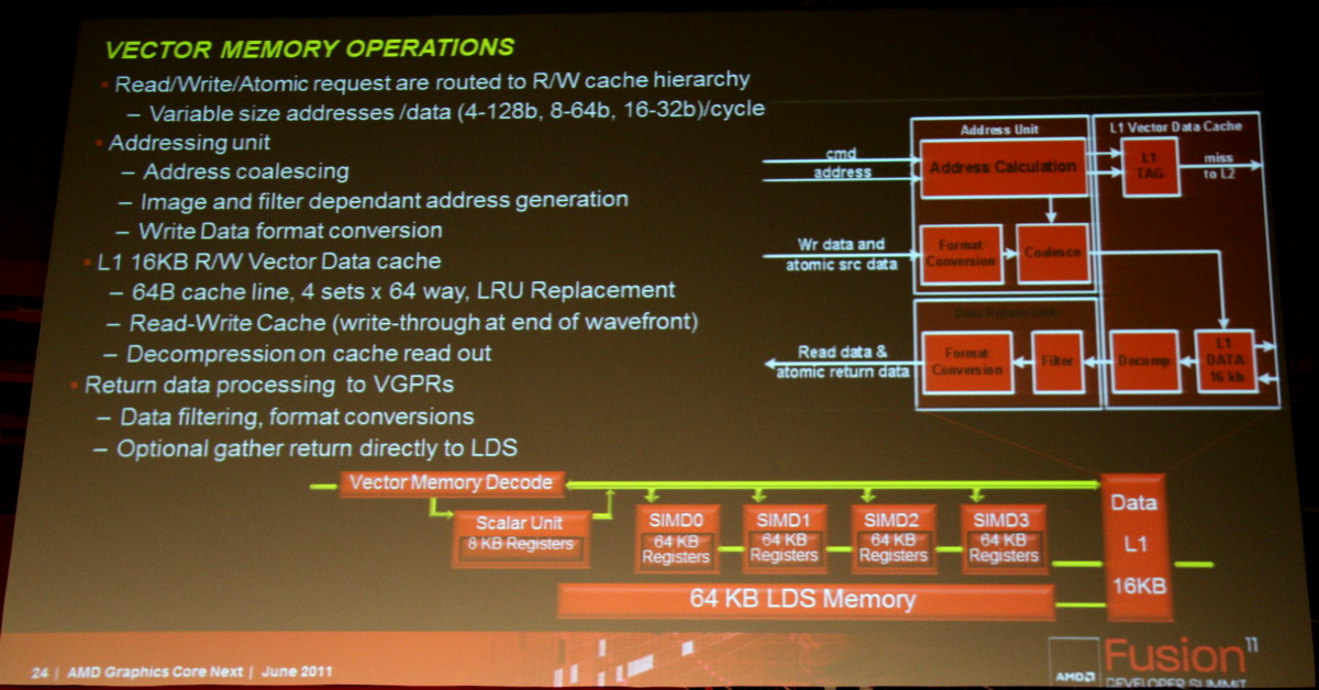
The poor choice is designing hardware assuming the maximum amount of memory is always needed.
Could you explain that assertion.
Follow along with the video below to see how to install our site as a web app on your home screen.
Note: This feature may not be available in some browsers.
The poor choice is designing hardware assuming the maximum amount of memory is always needed.
A CU is expected to much more denser than an SM.Fermi is also 64 FMA's per core clock. ALUs run at 2x core. A Fermi SM and a CU have the same throughput per core clock. Register file bandwidth per SIMD per clock is equivalent as well.
There will be a DX11.1 or 12.With respect to nVidia's response, there's no new API to shout about so they'll have to try harder.
In what sense does it take it another step further?
A CU is expected to much more denser than an SM.
A big feature that is being overlooked is coherency. It seems AMD will be offering full coherency while NV only offers semi coherent L1.
There will be a DX11.1 or 12.
So far:
Modularity - graphics and compute hardware are decoupled.
Parallelism - concurrent kernels from multiple application contexts.
I'd expect noise about that ~12 months before xb720.Oh, I haven't heard a peep about either.
How is that supposed to work with just 16 L/S units?128.
From the B3D's Fermi article:How is that supposed to work with just 16 L/S units?
16*4=64
Unless you are not referring to the clock those units run at (hot clock), of course.
The 16 LSUs run at hot-clock too, with all address generation happening here.
The cost of giving up VLIW ... and such a nasty cost it is.A CU can now do 4 threads from 4 different apps as well. I may have not grasped the idea fully, or correctly, but does any one else see a point in bunching different threads in to a CU? IMHO, MIMD over CU's would have been better than MIMD within a CU.
For a start, you can kiss your L1 goodbye, as each will get just 4K on average?
That is what I meant.From the B3D's Fermi article:
Just because it can be done, doesn't mean it needs to be or even will be done at all as default behaviour.A CU can now do 4 threads from 4 different apps as well. I may have not grasped the idea fully, or correctly, but does any one else see a point in bunching different threads in to a CU? IMHO, MIMD over CU's would have been better than MIMD within a CU.
For a start, you can kiss your L1 goodbye, as each will get just 4K on average?
The L1/LDS combo in Fermi runs at the base clock.That is what
Fermi-SM: 64 Bytes/hot clock aggregate bandwidth, 32 fma/ hot clock (or 48 fma/hot clock)
AMDs CU: 64 Byte/clock from cache/memory, 128 Byte/clock from LDS, 64 fma/clock
That does not matter for the flops/bandwidth question. One just has to use the same clock for flops/cycle and bandwidth/cycle that the division makes sense. If you take the base clock, the Fermi-SM would do 64 fma/cycle, the ratio does not change.The L1/LDS combo in Fermi runs at the base clock.
I think the compute core and the ff hw was decoupled earlier as well. What has changed in this context?
Cayman can do 2 kernels simultaneously.
That does not matter for the flops/bandwidth question. One just has to use the same clock for flops/cycle and bandwidth/cycle that the division makes sense. If you take the base clock, the Fermi-SM would do 64 fma/cycle, the ratio does not change.
Just because it can be done, doesn't mean it needs to be or even will be done at all as default behaviour.
The texture units (still a quad TMU, probably modified) are an integral part of the L1 cache block as can be seen here:Also texture units were coupled to a SIMD in Cayman, that's no longer the case.

So the comparison at Fermi's base clock:flops/clock and bandwidth/clock comparisons are easier when you're talking about similar clock speeds no?
What's changed is that they've caught up to Fermi in several important areas and those advantages actually matter now (and have been further generalized). Also texture units were coupled to a SIMD in Cayman, that's no longer the case.
The texture units (still a quad TMU, probably modified) are an integral part of the L1 cache block as can be seen here:
It was also mentioned explicitly in the talk about the fusion system architecture that there is the usual filtering hardware in there.
So the comparison at Fermi's base clock:
nvidia SM: 128 byte/cycle aggregate bandwidth, 64 fma/cycle (96 for GF104 type SM)
AMD CU: 64 byte/cycle cache/memory + 128 byte/cycle LDS bandwidth, 64 fma/cycle
I don't remember TMU organization being discussed. My guess is that TMU's are still coupled to a CU.
