AMD RDNA3 Specifications Discussion Thread

Right. Hence why I've said that it's there mostly for GCN compatibility (needed for consoles for the most part) and it remains to be seen if RDNA3 even expose "CU" in any capacity or just goes with "WGP" now as the basic shader processing unit.

In comparison Nvidia has "SM" which consists of 4 processing blocks with 2 SIMDs each all sharing the same L1/LDS. It is essentially the same design now in RDNA but with the capability to "split" WGP in halves to work in CU mode - which isn't really necessary for anything else but h/w level GCN compatibility?

Yeah I mostly have an issue with the confusing naming. The WGP is actually the CU. “CU mode” should really be called GCN compatibility mode. I wonder what mode compute shaders in games usually run under.

Why? That's the vector register file getting 50% increase.

Aside from the register and L0 cache increases and of course dual-issue SIMDs were there any other fundamental changes to the structure of the WGP?
 
Gosh, thanks for explaining the obvious stuff, what I am trying to tell you is different. How it scales depends not just on the yield of perfect dies, but mostly on how you bin chips for your products and on final products characteristics, isn't that obvious?
Well , you seemed to be surprised about the "obvious stuff" which is that 2x area costs more than 2x .I may have misunderstood your surprise, but that's why i said what i said..

Binning chips and redundancies are just that, another variable that can be accounted for statistically. In the end, it just enables to negate / mitigate the effect of a proportion of the defects. Of which you get more of ( per die) for bigger dies, hence why the non-linear increase of costs with area is maintained.
 
That's an interesting stuff given that smaller chips usually have more FE, display and other logic (relative to SMs and other blocks that can be disabled) that, if defective, would make a GPU unusable.
Still there is nothing one can't solve by adding a bit of redundancy and more flexible floorplanning (if this was a problem indeed).

There are defects beyond logic failures, such as shorts between ground and power. Such defects render a die completely unusuable no matter where on the die they hit. No amount of redundancy helps you if providing power supply causes the die to melt. These kinds of defects are much more common on modern processes than they were in the past, because of smaller line and dielectric widths in BEOL.
 
you seemed to be surprised about the "obvious stuff" which is that 2x area costs more than 2x
Of course, and I am still surprised with how some can pull the 2-3x factors for AD102 cost over the whole Navi 31 assembly out of their.. lets say heads for politeness, while not having any statistical data or even knowing yields of configurations used in real products.
 
Yeah I mostly have an issue with the confusing naming. The WGP is actually the CU. “CU mode” should really be called GCN compatibility mode. I wonder what mode compute shaders in games usually run under.
That’s one way to look at it.

But there are some known downsides to the WGP mode as well:

1. L0 is not workgroup coherent, so those will have to hit L2.

2. LDS throughput can be lower in some cases, due to LDS in WGP mode operating in some undisclosed “near-far” arrangement. My guess is the interleaving across the two 64KB arrays is not as fine grained as that within the array (each has 32 4-byte banks). They could be interleaved at LDS allocation granularity, given that AMD seems to claim a WGP can run workgroups of both modes concurrently.

Haven’t found out what heuristics are used to pick WGP mode or CU mode.

Aside from the register and L0 cache increases and of course dual-issue SIMDs were there any other fundamental changes to the structure of the WGP?
Apparently moving to software scoreboarding. Potentially more ways to dual-issue than just bundling instructions (e.g. single-cycle Wave64).

Otherwise I doubt so.
 
Last edited:
There are defects beyond logic failures, such as shorts between ground and power.
Yes, another obvious stuff, I can easily imagine shorts being a thing for failed packaging too, specifically when you need to physically align chiplets with micro precision (which feels like something a lot more error prone in comparison with on die interconnections).
 
Of course, and I am still surprised with how some can pull the 2-3x factors for AD102 cost over the whole Navi 31 assembly out of their.. lets say heads for politeness, while not having any statistical data or even knowing yields of configurations used in real products.
You know, rough estimates are permitted to a degree in discussions like these. They may be based on assumptions that are wrong but we'll never know, since we'll probably never have the full statistical data available.
But if say 2x the size used to cost 3x usually in other cases, with the data little data we've got, it's a good starting point to asume the same in this situation. While waiting for concrete points to correct that.

I find it silly to burry our head in the sands for this case, ignore similar past cases, discard our probably good intuition of the process just because we don't have the full accurate data.
 
Past cases (financial reports) point that NVIDIA has been enjoying much higher margins and 8-9x market share for a very long period of time all while having to dealt with "the disaster that was Samsung 8LPP":)

We're talking about manufacturing costs here, not margins and market share.

There is a host of other variables once you bring those too in, most with little correlation to manufacturing.
You can't have it both ways : complain about not knowing how the binning impacts yield percentages but then happily summoning other disciplines with many more unknowns into the discussion.
No ones knows the manufacturing costs only nvidia and amd know.. plus the consumer only buys whats being offerd by the vendor
 
Past cases (financial reports) point that NVIDIA has been enjoying much higher margins and 8-9x market share for a very long period of time all while having to dealt with "the disaster that was Samsung 8LPP":)

And that has absolutely what to do with fabrication of chips? I could certainly understand if the products that NV were selling were much much cheaper and thus much much more reliant on the cost of fabrication, but that's not the case.

RTX 4090's MSRP is 1600 USD with board partners allowed to sell their product for even higher than that. How much is it going to materially affect the margins if AD102 costs 2x or even 3x the cost of N33? Especially considering that NV can and will adjust the price that they sell those components to their AIBs (who will also adjust the price upwards if they feel they can) for in order to maintain their margins?

Regards,
SB
 
Have there been any leaks or indications of the price or performance of the RX 7800 XT? With AMD having the 6800 XT and 6900 XT so close in performance terms are people assuming that those 2 have been replaced by the two 7900 cards? Would the 7800 XT replace the RX 6800, and slot in at $550-650, with RX 6950 XT like performance?
 
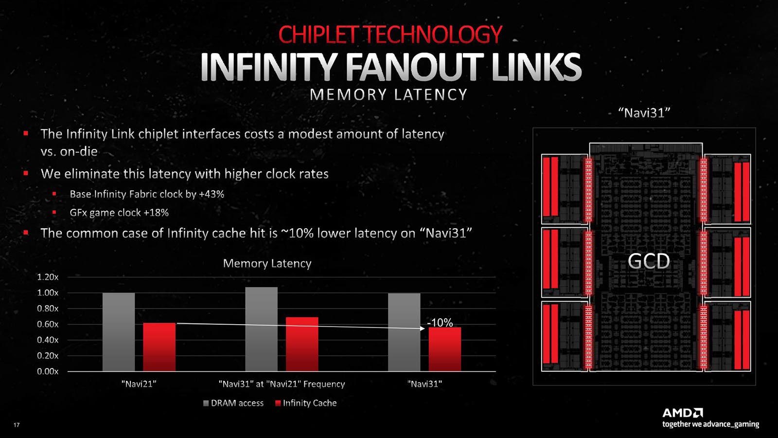
https://videocardz.com/newz/amd-rad...-bandwidth-density-than-ryzen-infinity-fabric

AMD-RADEON-RX-7900-NAVI-31-6.jpg
 
It would be interesting to know how much this chiplets interconnection does cost in terms of price and thermal, and if it's suitable for cpus too.
 
The picture of the "Infinity links with High Performance Fanout" showing clearly translucent layers increases my suspicion, that AMD does not use elevated fan-out bridges as first reported by some outlets, but indeed some InFO-R variant without a local silicon interconnect. It enables a way higher connection density for the redistribution layer compared to the routing over the package substrate and should be cheaper (but it consumes a bit more power than silicon bridges; the quoted 0.4pJ/bit would be on the very high end for relatively low clocked silicon bridge connections with a lot of lines).
 
Last edited:
Back
Top