AMD RDNA3 Specifications Discussion Thread

Maybe it was just a design goal. Doesn't mean they hit it.
Why would they want then to mention this here as achieving industry's 1st 3+ GHz despite of not being able to do that in reality?)
I can easily believe that front end part of the chip can hit the frequency (because competitor's much larger and more complex chip can already do this), but fixing power draw in "respin" without redoing design sounds like a bs.
Well the slide says "architected to exceed 3 ghz" so it could still be interpreted as a goal. I'm curious when we will find out what Bondrewd is hinting at as the wall they hit in development. I also hope we get some post launch interviews in December and someone asks them why they decided to go the dual issue route, curious to see the marketing spin for that one.
 
Why not put the ROPs on the MCDs as well? Dont' they usually benefit from being as close as possible to the cache and memory? Or maybe that's the L2 cache. I'm thinking back to the Xbox 360 GPU design.

Maybe moving this kind/amount of data cost to much energy ? Or latency ?
 
Why not put the ROPs on the MCDs as well? Dont' they usually benefit from being as close as possible to the cache and memory? Or maybe that's the L2 cache. I'm thinking back to the Xbox 360 GPU design.
Too much data traffic. You do a lot of hierZ and stuff in there.
 
So, did some napkin math (or rather napkin thoughts) with the following prerequisites (no matter how true or not):
- Frank Azor (i think in a full-nerd-video?) saying, 4080's the competition for XTX
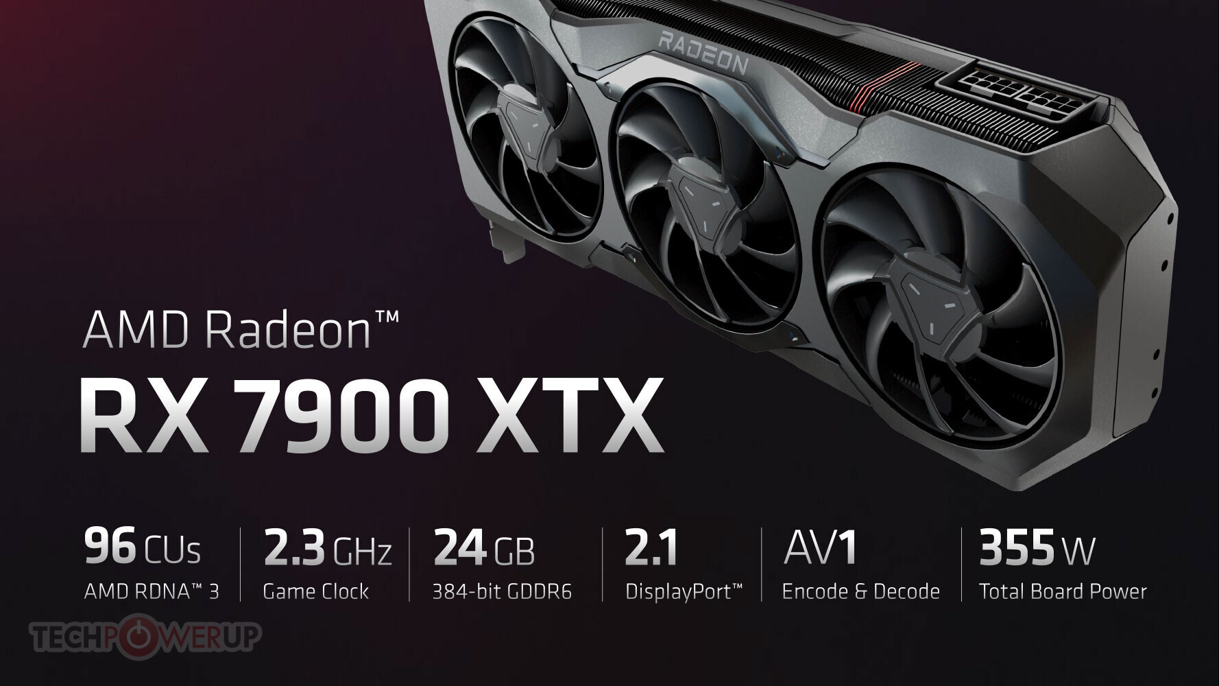
- XTX is the full blown chip, no hidden units
- clocks as is
- 300+6x37 = 522 mm² of N5/N6
- MCD packaging
- 384 Bit/20 Gbps 24 GByte G6
- 355 watts TBP

vs.
- AD103
- 378 mm² N4
- regular packaging
- 256 Bit 16 GByte G6X (no more reserves wrt to clocks)
- 320 watts TDP
- 5% reserve in SMs
- 10% reserve in TDP (for matching 355)
- reserves in TDP and SMs good for another combined 7.5% real world perf (each half of their numerical theoretical value)
- 4080 "ti": 4080*1,07

Could be a pretty close match overall, raster probably with an advantage for RX, RT for RTX (with likely a higher margin than raster for RX). DLSS2/3 better than FSR2/3, DP2.1 better than DP1.4a/DSC.

Great unknowns: Real world clocks under gaming load (4090 exceeds rated clocks by quite a margin, older RX6K did as well wrt gaming clock) and effectiveness of VLIW2 or rather shader compiler at this early stage.

Now I wonder, if AMDs BOM is significantly lower than Nvidias, making the move to chiplets right now not only an investment into the future, but a financial advantage as well. MSPRs notwithstanding, we know how much Nvidia loves and needs margins and how AMDs wants and needs to expand market share.
 
The RT uplift this new RDNA architecture gets may not be to the same level as Nvidia's 4000 series, but it's still a respectable jump from their previous line and it seems like their pricing and marketing properly reflects that reality.

Yeah a 1.8x improvement is more than respectable. Hopefully it means that AMD will encourage more impactful RT usage. I really wish they were more proactive about saying/showing how they think RT should best be used in todays games. But they’ve been acting a bit like Nvidia during early async compute days - pretending it doesn’t exist until they have something good to show. It’s not clear whether that’s just prudent marketing to avoid emphasizing a competitor’s advantage or if RT is truly considered unimportant inside AMD.
 
It’s not clear whether that’s just prudent marketing to avoid emphasizing a competitor’s advantage or if RT is truly considered unimportant inside AMD.
The former.
They'd be a bit less coy about RTRT if they didn't miss on clocks like hell.
Right now they run pretty decent SM deficit (96 vs 128, 60 vs 76 and so on and so forth) without any clk advantage to NV at each tier which impacts RTRT perf quite some.
 
Now I wonder, if AMDs BOM is significantly lower than Nvidias, making the move to chiplets right now not only an investment into the future, but a financial advantage as well. MSPRs notwithstanding, we know how much Nvidia loves and needs margins and how AMDs wants and needs to expand market share.

I would be skeptical that BOM is lower than AD103, if anything AD103 derived products you'd think would be cheaper (and RTX 4080 16GB isn't even fully enabled). I wouldn't even assume the silicon cost is cheaper before you factor in the packaging/board/memory/etc. BOM being lower than Nvidia was when AD102 was the comparative point in discussions.

For what it's worth Semianalysis's BOM estimates - https://www.semianalysis.com/p/ada-lovelace-gpus-shows-how-desperate

And the article frames Nvidia rather negatively. Interesting to note that this was also when the expectations that Navi 31 would be a AD102 competitor.

However unit cost's aside this does (well presumably) allow AMD to reuse the same MCD design over 2 chips and even more product configurations. This might save some fixed costs compared to developing two monolithic. But at the same time it's hard to say if this is a competitive advantage itself or just more just a better fit for AMD itself as we know AMD likely has to amortize fixed costs over less volume. Nor do we publicly have any idea what the fixed cost profile for these companies are.

But the above is just cost which is of course different from price. But just briefly, as this isn't really the thread for it, it's already been discussed how RTX 4080 (both variants before cancellation) was priced seemingly rather high just against the RTX 4090.

On the topic of chiplets my feeling on this for awhile in terms of public perception is that AMD's marketing focus on the subject and it's success against Intel's CPUs (being framed as chiplets vs. monolithic in the DIY space) has created this impression almost that they are some sort of panacea whereas the reality is much more complex.

Yeah a 1.8x improvement is more than respectable. Hopefully it means that AMD will encourage more impactful RT usage. I really wish they were more proactive about saying/showing how they think RT should best be used in todays games. But they’ve been acting a bit like Nvidia during early async compute days - pretending it doesn’t exist until they have something good to show. It’s not clear whether that’s just prudent marketing to avoid emphasizing a competitor’s advantage or if RT is truly considered unimportant inside AMD.

From a marketing stand point (and I don't just mean advertising) the approach actually makes sense. I know people like this romantic notion of general aggressive broad competition and fighting for market share but marketing to a specific segment of consumers also works. If there is enough of a raw rasterization performance numbers audience than it makes sense to narrow your focus and target them. To be honest AMD's strategy in general if you look back has been to target the "raw numbers" (for lack of a better term). Because ray tracing is viewed as a subset/add-on still it helps them in this regard compared to if it were actually rolled into the typical "max settings" standard for comparisons.
 
6600XT would net you ballpark console performance (PS5/XSX) in raster and RT. That gpu is probably good enough for most 'casual' gamers, while higher end gamers are not even having something that low-end on the radar to start with.
There are more arguments:
On PC you need a higher framerate because mouse causes much faster camera motion. 30fps feels often unplayable, while on console it's more acceptable.
Also, with similar HW, you'll get worse performance because PC lacks some optimization options (both SW and HW) due to being an open platform spanning variable HW requiring compromised APIs, reducing options and value of low level optimizations.

Thus you need a bit more powerful HW in general on PC to have a good experience with the same games, even if you're not an enthusiast aiming for high gfx settings.
 
The big question is if this bug changed changed the F/V curve at all, or if it's simply a F wall. If it's a F wall, then really nothing changed here beyond us not getting indoor heating. If they had to push V to get to the current Fmax, then that's a gigantic handicap in perf/W.
Yes, that's an important distinction. I don't think exceeding 3 GHz would matter if it required silly levels of power consumption, as the 7900 XTX is already a 355 W card. If the f/v curve is affected, the card would possibly be much worse than it could have been.
 
4dZf1DS0cksNlv4H.jpg


I REALLY like the design of that card. Looks sexy:yes:
 
The big question is if this bug changed changed the F/V curve at all, or if it's simply a F wall. If it's a F wall, then really nothing changed here beyond us not getting indoor heating. If they had to push V to get to the current Fmax, then that's a gigantic handicap in perf/W.
Should be the latter since quoted Phoenix PPW bumps are considerably more than what we've got in NV31, and PHX has no benefit of having a 20% WGP count bump or a fatter regfile.
 
Why not put the ROPs on the MCDs as well? Dont' they usually benefit from being as close as possible to the cache and memory? Or maybe that's the L2 cache. I'm thinking back to the Xbox 360 GPU design.

ROP is a screen-space construct these days, each of which owns sets of screen tiles that don’t necessarily map 1:1 to interleaved memory channels architecturally anymore. You get the benefit if there is locality to be exploited. Not much so in this case.
 
DP2.1 better than DP1.4a/DSC
UHBR 13.5 is just 54 Gbps, about 60% of DP 2.1 max spec and just 6 Gbps more that HDMI 2.1 FRL6 available starting with Ampere.
I honestly don't know why they've spent so much time on this "advantage" because it's hardly even an advantage.
 
UHBR 13.5 is just 54 Gbps, about 60% of DP 2.1 max spec and just 6 Gbps more that HDMI 2.1 FRL6 available starting with Ampere.
I honestly don't know why they've spent so much time on this "advantage" because it's hardly even an advantage.
What do you mean 'spent so much time'? It's slightly upgraded display controller, sure, but they were DP2.1 with Ryzen 6000 already (UHBR10 in that version), nothing in it suggests it took particularly much time.
Also the difference isn't 6 Gbps, datarate difference between HDMI FRL6 and DP UHBR13.5 is over 10 Gbps or 24.3% and it does allow clearly higher res/hz
 
Back
Top