Long before, given that it was ported lock, stock and barrel from the 32nm design.If I'm not mistaken, Dave has mentioned that Cayman taped-out in May. Most design decisions were probably set in stone long before that.
Install the app
How to install the app on iOS
Follow along with the video below to see how to install our site as a web app on your home screen.
Note: This feature may not be available in some browsers.
You are using an out of date browser. It may not display this or other websites correctly.
You should upgrade or use an alternative browser.
You should upgrade or use an alternative browser.
AMD: R9xx Speculation
- Thread starter Lukfi
- Start date
Long before, given that it was ported lock, stock and barrel from the 32nm design.
Then where did Barts come from? Who is Barts' daddy and what did he do? To use the famous Kindergarten cop line...
hoom
Veteran
I think the mosfet thing & the shaved power connector are probably one & the same.Yea that was another rumour, the TI mosfet thing. They claimed that the same component was also being used on the 68xx series but there was plenty of supply of those cards so i dont buy that rimour
A hint dropped by someone at ATI along the lines of
"There aren't enough of a particular component used by the power section"
")
Meaning
"PCIE power connectors that don't interfere with the fan"
But since misplaced/mis-sized dirt cheap plastic power connectors (or is it the shroud?) is the sort of fuckup you'd never expect to see, people presumed the problem to be in the more rare/expensive components like mosfets.
Long before, given that it was ported lock, stock and barrel from the 32nm design.
Interesting....so no SIMD cuts....i always wondered if AMD went with extra one-two SIMDs for each Caymans..would that make em more successful? How much die area does one SIMD cost, they are already 390mm what would going slightly past 400mm make em as uneconomical?
Oh but Cayman aint that bad... if going forward, more games use DX11 hw like Metro...i think Caymen will end up more well received...i am expecting Cayman to drop prices like RV790...not as fast as brutal but it well be better than Cypress...
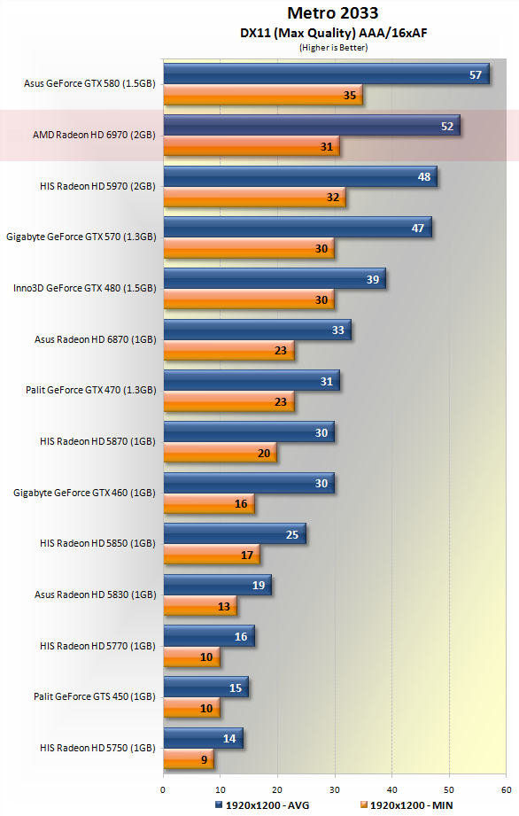
http://www.techspot.com/review/348-amd-radeon-6970/page10.html
hoom
Veteran
So Cayman 32nm would have had identical features/unit counts & they just redid it with the 40nm design rules? Or chopped some unit counts for size as well?Long before, given that it was ported lock, stock and barrel from the 32nm design.
So Cayman 32nm would have had identical features/unit counts & they just redid it with the 40nm design rules? Or chopped some unit counts for size as well?
What size would the chip be (about) if done at 32nm? I suppose that could give us some idea on wether there was any cuts made or not
It wouldn't have been the enthusiast grade chip at 32nm surely.
It shouldn't be either, the question would it be "sweetspot sized" or smaller than that, enthusiast is for 2 chips at AMD
What size would the chip be (about) if done at 32nm? I suppose that could give us some idea on wether there was any cuts made or not
For what it's worth, I believe scaling from 65nm to 55nm was 10% linearly on TSMC's process. This is supported by GT200b, which I think was around 460~480mm², while GT200 was 576mm². And 576 × (0.9)² = 466,56.
Assuming the same for 40->32, it would have been something like 389 × (0.9)² = 315,09mm², a bit smaller than Cypress.
"Lock, stock and barrel" sounds to me like no changes were made at all, which would explain Cayman's fairly high die size and power.
Though 40>32is bigger chance percentagewise than 65>55nm, 32nm is 80% of 40 while 55nm is nearly 85% of 65nm
If that nearly 5% difference translates more or less directly to chipsize scaling, we would end up with ~281mm^2 chip which is getting already quite small.
It could have been even a bit smaller. Scaling should be (40/32)^2 assuming everything roughly shrinks the same. 65nm->55nm might be worse because it was only a half node shrink, where more parameters stay the same.Though 40>32is bigger chance percentagewise than 65>55nm, 32nm is 80% of 40 while 55nm is nearly 85% of 65nm
If that nearly 5% difference translates more or less directly to chipsize scaling, we would end up with ~281mm^2 chip which is getting already quite small.
It could have been even a bit smaller. Scaling should be (40/32)^2 assuming everything roughly shrinks the same. 65nm->55nm might be worse because it was only a half node shrink, where more parameters stay the same.
So Cayman at 32nm would have been (as large as) Barts
Yeah, roughly. I think this could make some sense - this is also the same size as RV770 was. Plus we heard that 32nm was going to be more expensive per transistor (so even if you factor in the smaller die) than 40nm.So Cayman at 32nm would have been (as large as) Barts
I'm wondering though if anand knows more than we do (definitely had good information about Cypress, though only later IIRC). He hinted that apart from pcie 3 and some simds more stuff was dropped. Could have been pure speculation though - I guess pcie 3 could have got kicked earlier (too risky and unneeded for that timeframe). Also, after the experience with the transition to 40nm, I don't think anyone expected a smooth transition to 32nm - hence it might be possible that even if there were some more things on the wishlist for that chip, they were removed even before it was decided it has to be migrated to 40nm (and I don't think just more simds would have made any sense without other changes), just to keep the chip simpler.
Probably a bit larger as some parts (I/O) don't shrink well. I would guess roughly RV790 size.So Cayman at 32nm would have been (as large as) Barts
This from anandtech 6870,6850 review. http://www.anandtech.com/show/3987/...renewing-competition-in-the-midrange-market/2
So i think it works also the other way. And caymans MC-s are maybe fair bit bigger than cypress had.
So maybe the 32nm cayman midrange chip would have only those "Redwood" type MC-s and running on 4 GHz.
Along with selectively reducing functional blocks from Cypress and removing FP64 support, AMD made one other major change to improve efficiency for Barts: they’re using Redwood’s memory controller. In the past we’ve talked about the inherent complexities of driving GDDR5 at high speeds, but until now we’ve never known just how complex it is. It turns out that Cypress’s memory controller is nearly twice as big as Redwood’s! By reducing their desired memory speeds from 4.8GHz to 4.2GHz, AMD was able to reduce the size of their memory controller by nearly 50%. Admittedly we don’t know just how much space this design choice saved AMD, but from our discussions with them it’s clearly significant. And it also perfectly highlights just how hard it is to drive GDDR5 at 5GHz and beyond, and why both AMD and NVIDIA cited their memory controllers as some of their biggest issues when bringing up Cypress and GF100 respectively.
So i think it works also the other way. And caymans MC-s are maybe fair bit bigger than cypress had.
So maybe the 32nm cayman midrange chip would have only those "Redwood" type MC-s and running on 4 GHz.
Well, if you just do the calculation you end up with 250mm². Though yes not assuming everything shrinks perfect is probably a wise idea.Probably a bit larger as some parts (I/O) don't shrink well. I would guess roughly RV790 size.
Also, maybe it wouldn't have shrunk quite that well. I think TSMC 40nm is supposed to have gate pitch (which I believe is a fairly important parameter when it comes to transistor density) of 160nm, and the 32nm process was rumored to have gate pitch of 130nm. 160²/130² gives a very slightly worse ratio than 40²/32². (FWIW, the number I found for 28nm TSMC is 117nm gate pitch).
Unlikely, that was their sweetspot.So maybe the 32nm cayman midrange chip would have only those "Redwood" type MC-s and running on 4 GHz.
caveman-jim
Regular
Then where did Barts come from? Who is Barts' daddy and what did he do? To use the famous Kindergarten cop line...
Bart's Daddy is the same as Cypress' Daddy
Barts appeared because when 32nm was questioned, and 4 GPU's on 32 wasn't a good idea, the engineering boffins said "how about 5 gpu's on 40nm?" which nicely filled the 'sweet spot' gap with 'Cypress done right'
Hence we have EQAA as a Cayman only feature, in the 6900 series line up (and the rest got thrown a bone in the form of MLAA).
Ahh I guess that makes sense now.
BTW, what did Dave save this generation? Ever since the HD 48xx cards, the thing Dave has saved has remained a mystery.
Similar threads
- Replies
- 85
- Views
- 15K
- Replies
- 3K
- Views
- 699K
- Replies
- 1K
- Views
- 397K
- Replies
- 12K
- Views
- 2M
- Replies
- 6
- Views
- 6K