AMD: Navi Speculation, Rumours and Discussion [2019-2020]

Status
Not open for further replies.
[Looking at the slides from Computerbase.de]

It seems the main benefit AMD is talking about is that heavy VGPR allocation threads will run with much less idle time, so shaders that allocate 64 VGPRs or more will no longer kill throughput if they are memory-intensive too. (GCN with only 2 hardware threads due to high VGPR or LDS allocation is quite happy as long as ALU:MEM ratio is fairly high, e.g. 20:1).

The pain point with GCN when it was introduced was that it was more sensitive to ALU:MEM ratio than the old VLIW machines. So this is a big deal: AMD will spend less time advising developers to watch out for VGPR allocations. NVidia solved this, eventually, by giving developers more VGPRs.

I'm not a fan of 32-wide hardware threads, even if there is a nice mapping to the bits of a DWORD, because a "square" (8x8) is often really good for breaking down work, and there's no square with a 32-wide thread. But 64 is still an option and a slide implies that in Workgroup Processor mode there are twice as many VGPRs available to each work group. So that's pretty spiffy!

This sounds like a fun machine to program: translation, they've given us a new exciting coarse-grained switch to play with, making the combinatorial space for algorithm optimisation twice as big...

Also AMD talks vaguely about spin-up and spin-down timings being better with this new design: the wider SIMDs help with that and the significantly denser scheduling hardware and caches, seemingly with no scheduler sharing even within the CU, let alone across CUs, should make time lost to short-lived and/or high-VGPR allocation threads much better.

So yeah, this really is a new hardware architecture for the CUs, not far off the change from VLIW to scalar when GCN launched.
 
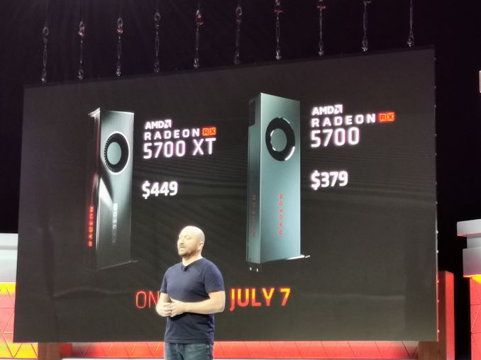
IMG_20190610_153946_575px.jpg
Is it me or does Chris Hook just look a whole lot different lately? :|
 

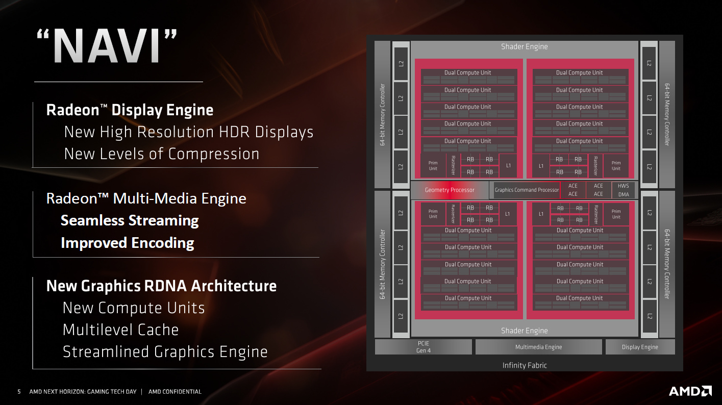
Assuming the two SEs are true here. There was an update to Apple Macbook pro Vegas last year, they had 20 CUs and only one shader engine. Assumedly this was some prototype for RDNA/5700, which now seem to have 20 CUs per shader engine

Nothing called "Arcturus" ever appeared on any AMD roadmap, ever.

Yeah my bad that was just rumors throwing that name around.
 
Assuming the two SEs are true here. There was an update to Apple Macbook pro Vegas last year, they had 20 CUs and only one shader engine. Assumedly this was some prototype for RDNA/5700, which now seem to have 20 CUs per shader engine
Look at the block diagram.
These are not SEs you're thinking of.
 
@Ryan Smith
When you do a review, can you make a beyond3d Suite Test of the 5700. I will be interested in the folowing values
0% Culling list
0% Culling strip
50% Culling list
50% Culling strip
100% Culling list
100% Culling strip

They did this on the German side with Vega64 and they get really curious data on the Frontend:
https://www.pcgameshardware.de/Rade...6623/Tests/Benchmark-Preis-Release-1235445/3/
What was the curious data for Vega64? It performs pretty close to 4 prims/clk.
 
seems pretty decent to me, a bit less money than the 2070, a bit more performance on average, cant really complain about that.

also remember navi was designed with scalability in mind so a bigger faster chip is going to be out sooner rather than later.

at any rate its finally coming out so we can all move on to speculating about the next big thing, and that's the real fun isnt it?
 
Look at the block diagram.
These are not SEs you're thinking of.

Big edit - Going over this again is slightly confusing. The block diagram clearly shows 2 shader engines. Each Shader Engine has 10 "Dual compute units".

16-1080.9ce6ffcb.jpg


Now are these dual compute units the mixed wavefront thing they're doing? So 1 "Dual Compute Unit" = 2 32 thread (stream processor) or 1 64 SP unit. If so then the 5700 would need two of the block diagrams shown to match the given numbers.

Or these dual compute units are 2 64 SP units, and the block diagram represents a complete 5700. I'm honestly not sure which one it is, the terminology doesn't match up here.
 
Last edited:
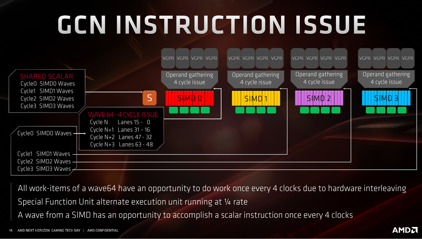
I'm confused about this slide about GCN:

21-1080.8d589ee0.jpg


The idea about a 4 cycle issue was that you could use cycle N to read 64x operand 0, N+1 to read 64x operand 1, N+2 to read 64x operand 3, and N+3 to write the result.

See also here.

The benefit of this scheme is that you don't need a multi-port RAM for the register file, and that you never have issues with bank conflicts (AFAIK, that's the case for GCN.) Yet that's not what this slide shows: it shows 4 register banks, and fetching the same operands for different lanes. If you do that, you might as well not have the 4 cycle issue?

Edit: OK, I'm a bit dumb... I'm right about the operands being fetched 64 at a time, but the SIMDs are being fed lane 0-15, then lane 16-31 etc. So it's as expected. The only thing still strange is that it shows 4 VGPRs as if there are 4 banks.

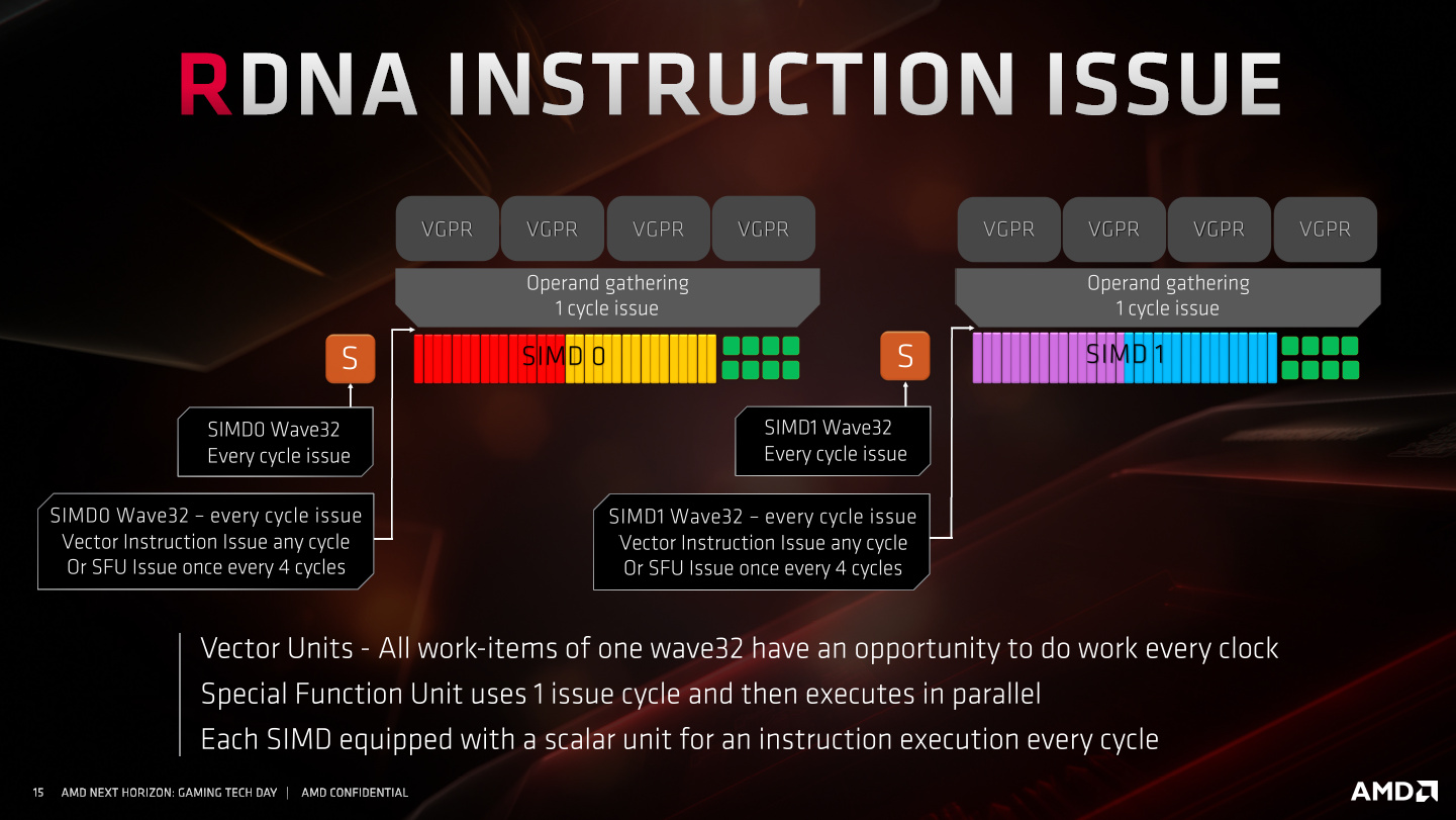
The RDNA slide makes sense to me:
22-1080.bf25e546.jpg


4 VGPR banks which allow single cycle issue... as long as you don't have bank conflict. That part of the architecture seems to be closely related to the Maxwell/Pascal SM (but not the Volta or Turing one.)
 
Last edited:
Status
Not open for further replies.
Back
Top