DmitryKo
Veteran
Hardly surprising considering the exact same CU/TMU count and memory bandwidth, and very similar boost clock and GT/s fillrate.About the same as 6950XT on average.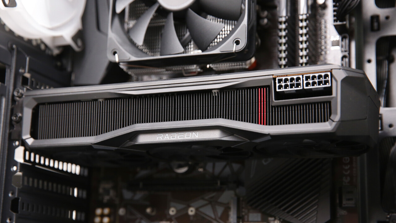
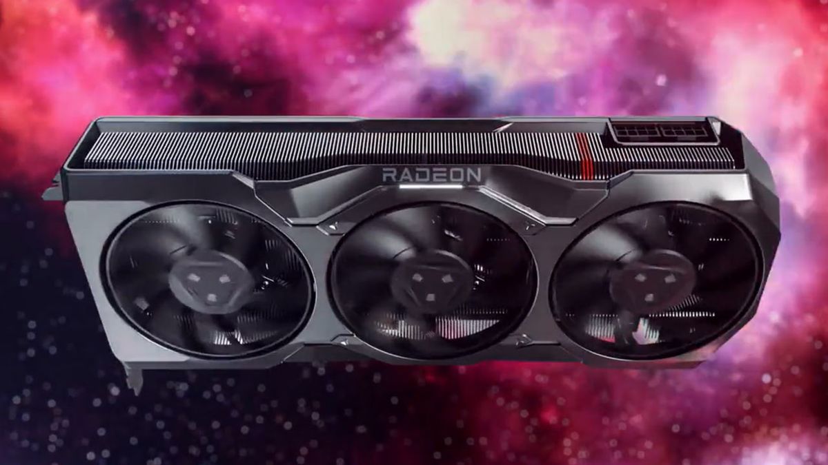
Die AMD Radeon RX 7900 GRE im Test
ComputerBase hat die Radeon RX 7900 GRE im Test. Sie zeigt eine Leistung auf dem Niveau der damaligen High-End-Grafikkarte RX 6950 XT.www.computerbase.de
Even in raytracing-heavy synthetic benchmarks like 3DMark Speedway, RX 6950 XT and RX 7900 GRE score about the same, while RX 7900 XT / XTX score 1.3 to 1.7 times higher, scaling with CU/TMU count, boost clocks, and memory bandwidth.
https://www.3dmark.com/compare/sw/122528/sw/758838/sw/300168/sw/550558/sw/209573/sw/306966
https://www.3dmark.com/compare/pr/2198884/pr/2485975/pr/2002278/pr/2044919/pr/2465595/pr/1948665
Exaclty. RX 7900 GRE is available to OEMs though - even Computerbase.de took their review card from a prebuilt PC - and typically you can find OEM parts at large retailers.That would mean having 3 different models within $150, seems a bit tight? While 7800 GRE isn't available in retail outside china, it does have official MSRP of $649
So RX 7800 XT would have little chance against RX 7900 GRE if it's only $50 cheaper, and RX 7700 XT would likewise struggle at double the price of RX 7600 for only 50% more performance.
With 7800XT naming, I expect around a $600 pricetag, which will only represent a very minor performance per dollar improvement from 6800XT. $550 could make it slightly more appealing, but I dont think AMD will do that.
I don't think RX 6800 XT pricing would apply to a much smaller die, when RX 7600 is already cheaper than RX 6600 (and actually the same as RX 5600 XT was). I'd rather expect mid-range RX 6750 XT / RX 6650 XT price levels for Navi 32.
I expect a ~52CU 7700XT to perform similar to a 6800 for about $500, again representing a minimal improvement in performance per dollar from previous gen.
My bet RX 7800 XT could be $549 to $499 if it's a 60 CU part, while RX 7700 XT could be $449 and probably as low as $399 if it's a 48 CU part.
[edit] A leak suggesting the same:
Last edited:
")