
Because it has 6 display pipelines. These both eat more ASIC power and each of the outputs need to provide more power as well.
You are using an out of date browser. It may not display this or other websites correctly.
You should upgrade or use an alternative browser.
You should upgrade or use an alternative browser.
AMD/ATI Evergreen: Architecture Discussion
- Thread starter Dave Baumann
- Start date
Whatever the reason HD5870 is sometimes ~20% slower than 2x5770, looks like something which should be improved. Be it internal bandwidth, limitations in thread dispatch, tri setup. So if that's not done in a cypress refresh, I'd expect it tackled in a new gen. That's not exactly sexy I guess. Obviously, more than 1 tri / clock could very well be on AMDs plate - even if it's true there's no benefit really for this generation, I think the expectation is tesselation will be used a a lot more hence there might very well be a benefit in the future.I'm sure there'll eventually be a thread devoted to this at some point but where exactly do you guys suspect AMD will go with their next architecture? Nobody expected Nvidia to tackle geometry head on, are there any other elephants in the room that AMD might want to take on?
With Cypress we've already seen that shaders, rops and texture units are providing rapidly diminishing returns yet we have folks claiming that bandwidth isn't a problem and geometry throughput isn't a problem. So what is it then?
Maybe make it even more programmable with less fixed function units (texture filtering, rops)? I can't see though quite how you'd get an improvement in perf/area for that right now (well, rv870 didn't improve on that neither, not that's a bad thing since it looks like even though fermi might have improved in that area from tesla it is still nowhere near Evergreen levels, except for vertex throughput).
If GPGPU is going to be more important, improving that might also be an option (that is, sustain DP mul/mad at half rate instead of a quarter of SP rate).
So far we have really no hints what direction AMD is going... Hints of future graphic APIs (d3d12?) would also help, but I haven't seen anything like that neither...
Jawed
Legend
L2->L1 in Cypress is, I presume, barely higher than in Juniper. Cypress's GDS is no bigger than Juniper's, I presume - GDS appears to be the linchpin of data movement during tessellation. GDS bandwidth is prolly no higher in Cypress than Juniper.Whatever the reason HD5870 is sometimes ~20% slower than 2x5770, looks like something which should be improved. Be it internal bandwidth,
Cypress should be 2x Juniper.limitations in thread dispatch,
Clearly no faster in Cypress than Juniper.tri setup.
I'm betting Cypress refresh will be as boring as HD4890 was.So if that's not done in a cypress refresh,
Yeah, as usual, Dave was being evasive. I think we can take that as admission that Evergreen is crap when tessellation hits hard (whatever the reason actually turns out to be). Just got to wait till GF100 appears to get decent confirmation of this.I'd expect it tackled in a new gen. That's not exactly sexy I guess. Obviously, more than 1 tri / clock could very well be on AMDs plate - even if it's true there's no benefit really for this generation,
If Evergreen is half-arsed D3D11, it'll be like the half-arsed DX9 (fp24) or lack of vertex texturing in SM3: "we deemed the die cost and performance not worth the bother at this time".I think the expectation is tesselation will be used a a lot more hence there might very well be a benefit in the future.
GF100 might be getting a very healthy boost in ROP performance from the L2 cache.Maybe make it even more programmable with less fixed function units (texture filtering, rops)? I can't see though quite how you'd get an improvement in perf/area for that right now (well, rv870 didn't improve on that neither, not that's a bad thing since it looks like even though fermi might have improved in that area from tesla it is still nowhere near Evergreen levels, except for vertex throughput).
GF100's cache hierarchy is also going to be highly advantageous in anything connected with compute.
Evergreen essentially can't do cached reads and writes to a single resource, as far as I can tell. You can either read it or write it and have caching, but not both. Atomics are accelerated via GDS, as far as I can tell, which is a partial solution, if your algorithm is atomic-happy.
DP/mm² is fine with ATI currently, I don't see any need for that to change.If GPGPU is going to be more important, improving that might also be an option (that is, sustain DP mul/mad at half rate instead of a quarter of SP rate).
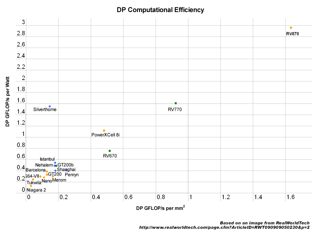
I suppose I should plonk GF100 on there. What is it? 448 SP ALUs at half rate, 1400MHz at 280W on 550mm²? So, erm, coordinates of 1.1 and 2.2?
I think there's little left to do with D3D12. WDDM needs to get fine-grained context switching, and compute needs to support task parallelism and arbitrary pipeline definition (i.e. producers/consumers + buffers/queues allowing them to communicate). Fermi appears to be further along.So far we have really no hints what direction AMD is going... Hints of future graphic APIs (d3d12?) would also help, but I haven't seen anything like that neither...
It'd be interesting to spend some time understanding how far ATI can currently go with its virtual function support and multiple concurrent kernel support.
Jawed
Jawed
Legend
No, there are key areas in Cypress that look over-stretched, e.g. L2->L1 bandwidth. While RV770 looks like it could scale up it's clear that Cypress didn't scale everything up. Obviously we can't be sure that Cypress has reached the limit, but I think L2->L1 hitting the endstops like that is a clue.Don't forget, they can increase die area by 50% and still be smaller than NV. They can increase power use by 50% and still be smaller than NV. Given that they have a VERY modular architecture, neither would be much of an engineering problem.
One of the key problems here is identifying the scaling problems in Evergreen. As far as I can tell near enough zero investigation has been done by any website.
Jawed
I haven't seen any numbers for juniper, but cypress was stated as having same (per clock) l2->l1 bandwidth as rv770, so it seems a fair assumption juniper is the same too.L2->L1 in Cypress is, I presume, barely higher than in Juniper. Cypress's GDS is no bigger than Juniper's, I presume - GDS appears to be the linchpin of data movement during tessellation. GDS bandwidth is prolly no higher in Cypress than Juniper.
Yes, but I'm told for things like http://www.guru3d.com/article/radeon-hd-5770-review-test/16 it is not setup limited. Despite not 100% scaling of Crossfire (though arguably scaling is good in this test) the HD5870 is a lot slower than 2x5770 (in fact the 5850 is terrible compared to previous gen too). I don't think GDS plays a part here neither. But something like a 30% loss just due to internal bandwidth restrictions? What else?Clearly no faster in Cypress than Juniper.
So you think it's not going to be a true chip refresh (functional logic exactly the same, just like what was the case for rv790)? Boring indeed. I'm not convinced though, at least not if HD5890 even features a new chip.I'm betting Cypress refresh will be as boring as HD4890 was.
Yes, it is certainly fine. But if you'd think DP is as important as SP, then it would make sense to upgrade that probably. After all pretty much all modern cpus have half rate muls. The cost (of the beefed up multipliers, basically) is of course significant, but still half rate makes sense (as operand fetch rate for instance is the same as full rate SP requires). Though at this point DP probably really isn't that important...DP/mm² is fine with ATI currently, I don't see any need for that to change.
FrameBuffer
Banned
Because it has 6 display pipelines. These both eat more ASIC power and each of the outputs need to provide more power as well.
Correct me if I am wrong but aren't the HD5000 series limited to 4 outputs per GPU.. yet the 5870 (6) is s single GPU.. does this mean that 2 additional DP were "tacked on" ? Any chance of seeing DP 1.2 compatible ports (at least from the 2 "extra" ports) ??
((I know .. I know.. you can't talk about unreleased/unannounced products with fears about giving important information to your competitors))
Last edited by a moderator:
No Cypress, Juniper and Redwood have 6 display controllers. Cedar has only 4 though.Correct me if I am wrong but aren't the HD5000 series limited to 4 outputs per GPU.. yet the 5870 (6) is s single GPU.. does this mean that 2 additional DP were "tacked on" ? Any chance of seeing DP 1.2 compatible ports (at least from the 2 "extra" ports) ??
I don't think though OEMs are allowed to make cards with more than 3 independent outputs (if you look at the specs at the AMD site, it always says "3 independent display controllers", except for mobile parts).
Related to GF100 I did a readup on the setup/rasterizer stage of Cypress and looking at the diagram at page 8 here http://sa09.idav.ucdavis.edu/docs/SA09_AMD_IHV.pdf
Seems like triangle setup is filling a buffer (1 tri/clock) from which each rasterizer can read (1 tri/clock each) and then setup fragments (16/clock each).
Now, what happens if I just submit a single fullscren pixel-heavy triangle - would half the chip be left idle then? Seems like it from the diagram, with each rasterizer supplying half the array.
(Could be even worse for GF100 with the 4 GPCs - ie. half rate in the much more common fullscreen quad case)
OpenGL guy
Veteran
On Cypress, if you're doing a full screen quad, both rasterizers would be fully utilized equally. Otherwise we wouldn't achieve peak (barring bandwidth constraints) fillrate in simple things like the 3DMark fillrate tests.Related to GF100 I did a readup on the setup/rasterizer stage of Cypress and looking at the diagram at page 8 here http://sa09.idav.ucdavis.edu/docs/SA09_AMD_IHV.pdf
Seems like triangle setup is filling a buffer (1 tri/clock) from which each rasterizer can read (1 tri/clock each) and then setup fragments (16/clock each).
Now, what happens if I just submit a single fullscren pixel-heavy triangle - would half the chip be left idle then? Seems like it from the diagram, with each rasterizer supplying half the array.
(Could be even worse for GF100 with the 4 GPCs - ie. half rate in the much more common fullscreen quad case)
Yes, a quad would be 2 equally sized triangles, and all fine (for Cypress at least, GF100 would have to do something).
But a single triangle big enough to fill the whole screen?
I know it's not common, but I've seen ppl doing it for fullscreen rendering - it can also prevent the occasional shading issues on the edge otherwise crossing the screen.
But a single triangle big enough to fill the whole screen?
I know it's not common, but I've seen ppl doing it for fullscreen rendering - it can also prevent the occasional shading issues on the edge otherwise crossing the screen.
Last edited by a moderator:
OpenGL guy
Veteran
It's not a problem as I stated above. Both rasterizers would be fully utilized.Yes, a quad would be 2 equally sized triangles, and all fine (for Cypress at least, GF100 would have to do something).
But a single triangle big enough to fill the whole screen?
I know it's not common, but I've seen ppl doing it for fullscreen rendering - it can also prevent the occasional shading issues on the edge otherwise crossing the screen.
It's not a problem as I stated above. Both rasterizers would be fully utilized.
Ok, so if the incoming triangle is "large" the primitive assembly will produce several smaller primitives for the buffer? And then the two rasterizers will grab these (sub)primitives and send the fragments to their respective Dispatch Processor, with no sharing / buffering between the DPs.
We also have the (opposite) problem of very small triangles, as speculated by Jawed here: http://forum.beyond3d.com/showthread.php?p=1382181#post1382181
Ie. whether a single hardware thread / wavefront can contain fragments from more than one triangle. Otherwise we could become very shader limited by drawing single/few-fragment triangles.
OpenGL guy
Veteran
No, it doesn't work that way.Ok, so if the incoming triangle is "large" the primitive assembly will produce several smaller primitives for the buffer? And then the two rasterizers will grab these (sub)primitives and send the fragments to their respective Dispatch Processor, with no sharing / buffering between the DPs.
The triangle isn't subdivided so it fits. The surface is evaluated via edge equations to figure out where it touches a screen pixel, whether the edge lies inside or outside the pixel or not. Repeat for testing the next pixel, sharing data with the previous test because it's the same triangle.Ok, so if the incoming triangle is "large" the primitive assembly will produce several smaller primitives for the buffer?
But somehow the 2 rasterizers can share the work on large triangles, while when they are very small they can both consume a triangle/whatever from the buffer each clock.
The rasterizers could be working on their own small alternating screen tiles, so large triangles will end up buffered for both rasterizers (just one entry per triangle), while small will have a chance to stay within one tile. That would also solve the synchronization issue. I could imagine something like 8x8 or 16x16 - could be a driver profile option. Would be easy to test.
But that should all be part of the work done by one of the two rasterizers.
The rasterizers could be working on their own small alternating screen tiles, so large triangles will end up buffered for both rasterizers (just one entry per triangle), while small will have a chance to stay within one tile. That would also solve the synchronization issue. I could imagine something like 8x8 or 16x16 - could be a driver profile option. Would be easy to test.
The triangle isn't subdivided so it fits. The surface is evaluated via edge equations to figure out where it touches a screen pixel, whether the edge lies inside or outside the pixel or not. Repeat for the next pixel, sharing data with the previous one because it's the same triangle.
But that should all be part of the work done by one of the two rasterizers.
(I see we have the same thing going on (on cypress, not fermi) in two threads at the moment - merge pls ") )
)
Could it be one fat rasterizer with a special shortcut to consume 2 triangles per clock, if contained within 2 different tiles - and then AMD likes to talk about it as 2 rasterizers
)Could it be one fat rasterizer with a special shortcut to consume 2 triangles per clock, if contained within 2 different tiles - and then AMD likes to talk about it as 2 rasterizers
A depth intersection?I expect everyone is doing rasterization through parallel intersection tests of tiles nowadays, only using the traditional scanline algorithm to determine covered tiles.
Similar threads
- Replies
- 124
- Views
- 10K
- Replies
- 68
- Views
- 16K
- Replies
- 121
- Views
- 15K