IIRC it's the "Apple chip" aka Vega with 20 CUs40CU being the first navi chip as well, certainly looks like they had a decent source. I didn't pay much attention to that single shader engine chip, any pointers?
Install the app
How to install the app on iOS
Follow along with the video below to see how to install our site as a web app on your home screen.
Note: This feature may not be available in some browsers.
You are using an out of date browser. It may not display this or other websites correctly.
You should upgrade or use an alternative browser.
You should upgrade or use an alternative browser.
AMD: Navi Speculation, Rumours and Discussion [2019-2020]
- Thread starter Kaotik
- Start date
- Status
- Not open for further replies.
DmitryKo
Veteran
Sure, but did anyone ever try to identify and label out the functional blocks in a Compute Unit on the actual die shot? Things like LDS/registers/TMUs etc.there is some risk in using an conceptual diagram to guess at physical dimensions
Looks almost impossible to me without some inside information, since logic blocks are spread across all silicon-copper layers to maintain power and thermal limits, and the visible layer only reveals parts of these blocks but there is probably not enough information to reconstruct the entire CU .
The single official photo of a GCN die I could find is a functional diagram in the AMD Polaris whitepaper, with a grid of superimposed green squares standing in for CUs, but these don't even try to match the real Polaris10 die - though it does match what's visible of the real silicon like memory channels and I/O (for the most part, as the right edge is differrent).
Last edited:
http://chipsleuth.com/tahiti.html#annotated-rams-overviewSure, but did anyone ever try to identify and label out the functional blocks in a Compute Unit on the actual die shot? Things like LDS/registers/TMUs etc.
Looks almost impossible to me without some inside information, since logic blocks are spread across all silicon-copper layers to maintain power and thermal limits, and the visible layer only reveals parts of these blocks but there is probably not enough information to reconstruct the entire CU .
The single official photo of a GCN die I could find is a functional diagram in the AMD Polaris whitepaper, with a grid of superimposed green squares standing in for CUs, but these don't even try to match the real Polaris10 die - though it does match what's visible of the real silicon like memory channels and I/O (for the most part, as the right edge is differrent).
This guy is great. He's got a Tahiti article focused on CU and a Fiji one about the whole chip.
D
Deleted member 13524
Guest
So apparently the RX 5700XT does ~2150MHz average on 250W by tuning the power tables and placing the vcore at 1.25V (up from 1.2V default):
In the meantime, with undervolt to 0.966V the card consumes slightly above 130W while clocking 40MHz lower.
Plus, the drivers still don't allow any memory overclock so there might be some headroom there too.
It will be interesting to see what the third parties can do with open air coolers and custom voltage tables.
with undervolt to 0.966V the card consumes slightly above 130W while clocking 40MHz lower.
D
Deleted member 13524
Guest
AMD really likes their tradition of needlessly overvolting all their graphics chips out-of-the-box, I guess.
¯\_(ツ)_/¯
At least now they all have the automatic undervolting option in the drivers which when working with Navi should provide a very decent reduction in power consumption.
Though unless they enable it by default for Navi cards, I wonder how many of the average Joes are ever going to tick that box.
Some driver bugs and the driver doesn't play well with Handbreak (nor x264 GPU accelerated encoding, AMD is working on it since a few days back) atm but other then that it's trading blows with a Nvidia 2080 for Resolve, Premiere, Da Vinci Resolve & Handbrake
Value for performance is emphasized a lot.
DmitryKo
Veteran
That's sure interesting, even though the top layer only hosts SRAM in each CU.
Ive had a gcn card since 2012 and never even knew this was a thing.
Last edited:
 tested it out though, pretty good for animation, especially anime and fast moving scenes or sports
I've seen various attempts over the years (including the site linked in a later post). I think reverse-engineering companies like Chipworks (now part of Techinsights?) would have more certain breakdowns--but those don't come cheap.Sure, but did anyone ever try to identify and label out the functional blocks in a Compute Unit on the actual die shot? Things like LDS/registers/TMUs etc.
My running assumption for something like Polaris, based on various attempts at dissecting the CU:
Starting from the midline of an SE and going out:
L1, Load/Store, Filtering, SIMD 0 and SIMD1, LDS and scalar, shared front end (scalar cache, instruction cache, etc.), SIMD 2 and 3.
The supposed branch/message unit might be somewhere in the area the scalar and front end, I'm not sure. There are also things like wavefront instruction buffers whose position isn't clear to me.
I think the LDS is past the first set of SIMD blocks and before the front end because there's SRAM roughly in the shape and capacity as a register file, but not part of the SIMD blocks.
Generally a unit of some kind is going to try to have a relatively contiguous 2D footprint (don't want more distance for signal travel if not necessary), although with automated synthesis the exact boundaries get pretty blobby. There's only one layer of active transistors, with the rest being interconnect and elements like power planes and inductors/capacitors. While there are concepts with more than one transistor layer, at least traditionally the electrical properties of layers besides the single layer that was cut from the mono-crystaline ingot have been too poor to be justified with most chips and workflows.Looks almost impossible to me without some inside information, since logic blocks are spread across all silicon-copper layers to maintain power and thermal limits, and the visible layer only reveals parts of these blocks but there is probably not enough information to reconstruct the entire CU .
Manually designed blocks or blocks with some manual guidance or customization tended to be more common in older chips, and so their floorplans and units tended to have much more visible boundaries and paths. It's more difficult now because the paths and units are much smaller relative to the images we have, and without more domain-specific knowledge there are fewer obvious landmarks in the seemingly chaotic synthesized blocks.
So out of the box this thing does not ramp the fan over 43% so for my case which is pretty well ventilated i was getting 91 degrees and 110! Junction temp at 100% load. After some tweaking its staying below 90, but imagine it was in a shitty dell pc or something no bueno.
https://www.tomshardware.com/news/asrock-radeon-rx-5700-challenger-amd-graphics,39967.html
Asrock show off their custom 5700 cards.
My main concern with custom cooled cards is whether the heatsink/heatpipes make full contact with the die and aren't just carry-overs designed for nvidias larger dies. This happened with many 290/X cards from vendors that sold both AMD and Nvidia.
I guess one way to hopefully be sure before reviews are out is to buy Sapphire and the like, AIBs that only sell AMD.
As long as the die is roughly at the center between the mounting screws, I cannot understand how a heatsink's contact area would not make full contact with a smaller die than it was designed for. Contrarily, there would be a larger margin for error on the sides.My main concern with custom cooled cards is whether the heatsink/heatpipes make full contact with the die and aren't just carry-overs designed for nvidias larger dies.
Classic bad example: https://www.computerbase.de/2013-12/asus-radeon-r9-290x-directcu-ii-oc-test/2/#abschnitt_der_kuehlerAs long as the die is roughly at the center between the mounting screws, I cannot understand how a heatsink's contact area would not make full contact with a smaller die than it was designed for. Contrarily, there would be a larger margin for error on the sides.
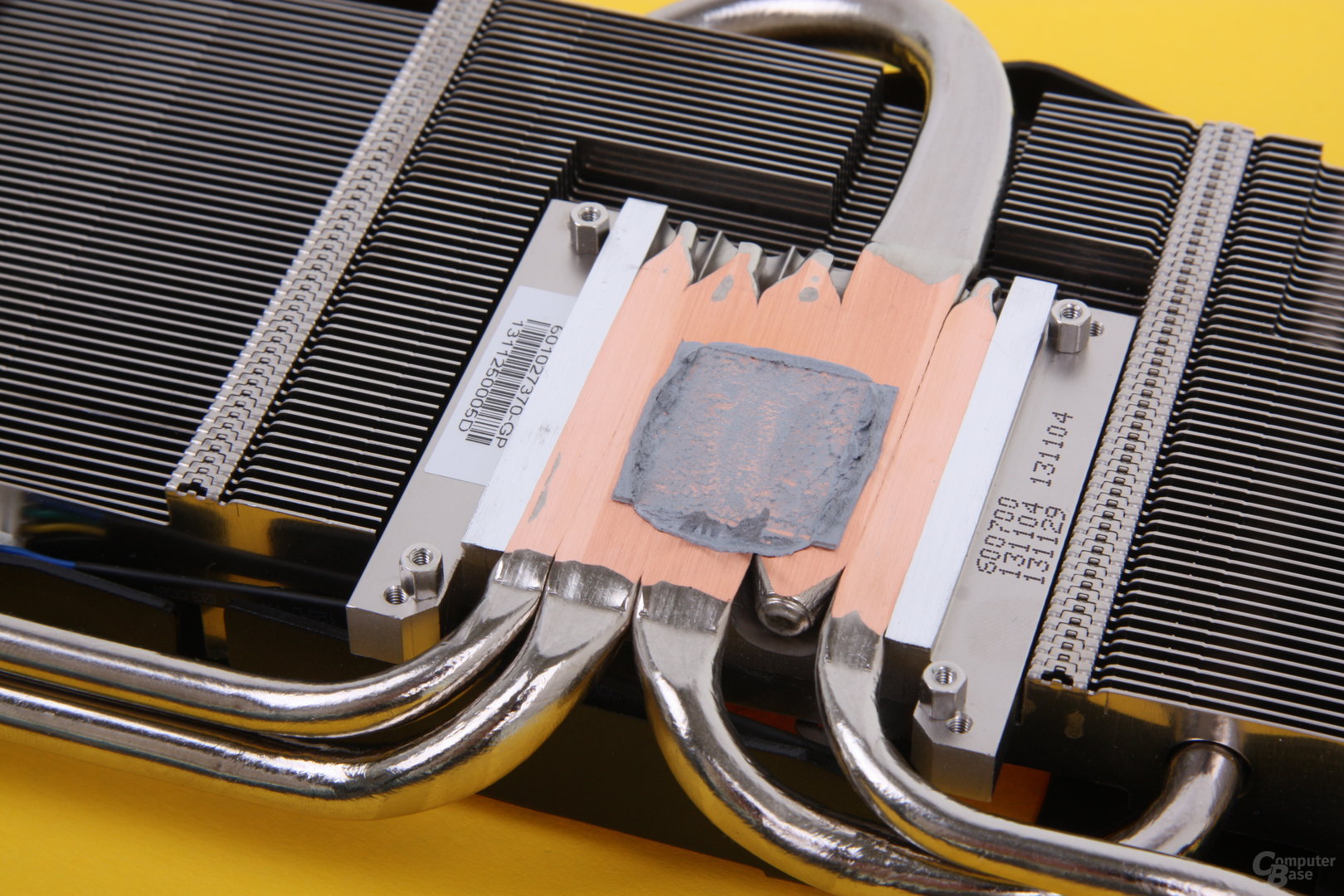
Yeah, that's excess heatpipes (the die even seems to touch the three larger heatpipes), so the cooling could be cheaper, but not better with a tailored heatsink. I was under the impression, RedVi was talking about bad cooling performance and thus higher noise levels.
Cooling performance on that card was pretty bad compared to the competition. Not surprising since the thermal connection to the two outer pipes - and corresponding parts of the fins - must be pretty bad. But I agree that if it was all encapsulated in a copper block instead of being direct touch it shouldn't matter too much.
That's the example I was thinking of Psycho. I Hope those designs are a thing of the past as from memory the thermal performance of that Asus 290X was quite bad compared to other designs. I was reminded of it because I have a 290X and because of there again being significant die area difference between AMD and Nvidia for the same tier parts.
Not sure if this should be in here, some Radeon Software thread or where, but this little snippet has been dug out from 19.7.2 drivers:
- Status
- Not open for further replies.