
My understanding was discrete GPUs at the end of the year and integration to the successor of Trinity in H2/2012, probably more towards the end of 2012. Perspectively, they aim to reduce the delay between discrete and APU to about 6 months.We were told directly by Eric Demers that the first products using this technology will be released in Q4 of this year. But it looks like on the APU side that Trinity is based on the VLIW4 of the Cayman chips. So, it could be another 1.5 to 2 years before we see this technology on the APUs.
You are using an out of date browser. It may not display this or other websites correctly.
You should upgrade or use an alternative browser.
You should upgrade or use an alternative browser.
AMD: Southern Islands (7*** series) Speculation/ Rumour Thread
- Thread starter UniversalTruth
- Start date
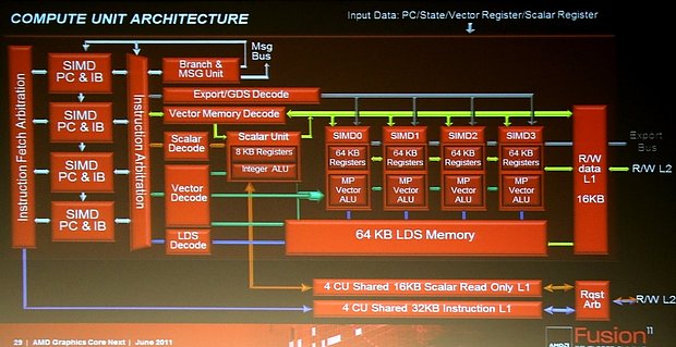
It's round-robin amongst the SIMDs, and then it picks amongst the ~10 wavefronts on a SIMD in that cycle.
Its 40*4 or 160 cycles before you potentially need to worry about the next instruction, and that's only if all other wavefronts are stalled. (edit: to clarify, if all the other wavefronts issue once and then stall after the instruction issue in question)
Are you sure? Each SIMD sees a new instruction every 4 cycles and it has 10 wavefronts to choose from. Hence 40 cycles of latency hiding. Or are all 40 wavefronts available to each SIMD for issue?
As I said already, you still have to track memory dependencies of course. You just don't have to care about dependencies between arithmetic instructions anymore. That basically reduces the dimensionality of a scoreboard to a score line. Appears simpler to me")
Ok, makes sense.
Are you assuming all 10 Wavefronts per SIMD are issuing memory operations and can't continue until they complete (because the next arithmetic instruction accesses the destination register of a pending memory instruction) at the same time and no wavefront is left doing some calculations?
No, I assumed the round-robin issue applied to the 10 wavefronts as well as the SIMDs. If each cycle you can fetch an instruction from any of the 10 wavefronts then all is well.
Afaik, Fermi is at 18 cycles for single precision instructions done on the vector ALUs. It isn't that bad.
Hmm, I remember seeing several references to 18 warps per SIMD being the minimum for guaranteed full utilization hence the 36 cycle claim.
That would mean that in absolute terms FSA can hide more latency time (because clockrate is significantly lower)?
Yep, I guess so.
Btw., I really think one has to give AMD some credit for naming things what they are. No stupid "scalar" ALUs (besides the one which is really scalar
That's cause you're viewing it in light of what has already transpired. Think of how ridiculously boring and uninformative it would have been if G80 was marketed as having "vector ALUs" back in 2006. Everything was already vector back then. It only seems mature now after you've been through 5 years of CUDA marketing
So are we looking at a AMD GPU that's doing to have hugely more transistors to only somewhat move beyond Cayman graphics performance? Similar to giant Fermi competing with significantly smaller Cayman and also GT200 vs. RV770. Essentially lots of transistors going towards a more GPGPU oriented, less graphics oriented design.
It's interesting to see graphics and GPGPU continue to diverge because it's not entirely clear that we consumers gain anything. How about future consoles? Maybe Xbox 3 will be VLIW4 or 5 to keep graphics focus and be smaller.
I'm waiting on the next ultra gimpy low-end GPU. NV's low end stuff certainly has suffered up against AMD's more graphics oriented architecture.
Are you sure? Each SIMD sees a new instruction every 4 cycles and it has 10 wavefronts to choose from. Hence 40 cycles of latency hiding. Or are all 40 wavefronts available to each SIMD for issue?
I think you're right. I was going through it in my head and wasn't overlapping the cycles of execution for the various SIMDs.
That looks to early for me it would mean the APU using it would appear at nearly the same time as the GPU - I thought Brazos update could just have basically integrated Caicos. OTOH though why not? The cpu core is pretty simple anyway.We were told directly by Eric Demers that the first products using this technology will be released in Q4 of this year. But it looks like on the APU side that Trinity is based on the VLIW4 of the Cayman chips. So, it could be another 1.5 to 2 years before we see this technology on the APUs. Now, having said that, I am curious if the Brazos update will not in fact utilize the FSA?
As for Trinity I'm wondering how CF is supposed to work there if no other VLIW4 gpus will appear? Just really asymmetric? Second cpu socket?
This is some fantastic news from AMD... now if MS will only support concurrent contexts sooner rather than later...
On anandtech, the author speculated they may stick with VLIW4 for the low end (short term), but I'd rather they just make the move forward and orphan Trinity. I mean is the CF market for that really important?mczak said:As for Trinity I'm wondering how CF is supposed to work there if no other VLIW4 gpus will appear?
Well I'm not a big fan of it but AMD put quite some emphasis on it seemingly. But that doesn't meant they can't just drop it againOn anandtech, the author speculated they may stick with VLIW4 for the low end (short term), but I'd rather they just make the move forward and orphan Trinity. I mean is the CF market for that really important?
. Or make it work with arbitrary gpus, it should certainly be doable just requires some effort.That looks to early for me it would mean the APU using it would appear at nearly the same time as the GPU - I thought Brazos update could just have basically integrated Caicos. OTOH though why not? The cpu core is pretty simple anyway.
As for Trinity I'm wondering how CF is supposed to work there if no other VLIW4 gpus will appear? Just really asymmetric? Second cpu socket?
Im thinking the same thing, the brazos update should be using Caicos. Hopefully they'll have certified the memory controller to use DDR3-1600 (Im assuming they'll stick to single channel mem controller). Along with higher clocks, overall graphics performance should be up at least 50-60% on Brazos.
As for the the successor for Trinity in H2 2012, well when is trinity supposed to be out? Q2 2012 at the earliest? After that im guessing they'll design the next APU for 22nm in mid 2013. Does it even make sense to design yet another 32nm APU after Trinity?
As for Trinity I'm wondering how CF is supposed to work there if no other VLIW4 gpus will appear? Just really asymmetric? Second cpu socket?
With aCF, different ISA's should be among the lesser of your worries.
Anand reviews show that aCF is far from ready atm.
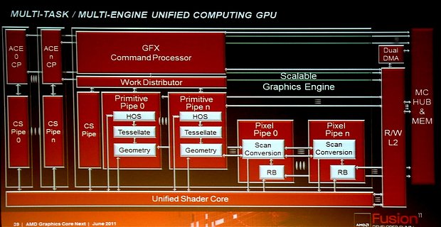
Complete GPU. The shader core at the bottom is comprised of the CUs (all of them, not a single one).Does anyone know if the graphics representation on page 20 of Eric Demers' presentation is for one CU or for a whole chip? I would tend towards the latter, but I am not entirely sure.
As CUs will form groups of 4, maybe each of those groups will resemble a GPC with its own primitive and pixel pipe (labeled wrong in the pdf of Demers). But maybe it's more decoupled.
Edit:
With the additional CS pipe and the (optional?) ACEs, it's probable it will be decoupled from the CU groups.
Edit2:
Compare with this slide from the other talk:
Last edited by a moderator:
In that case it wouldn't be shared anymoreThanks, but what makes you think the CUs will be grouped into quads? The mentioning of „4 CU shared memory/L1”? I am actually wondering if that „4” should really read as four or rather as for, i.e. intra-CU.
It really means 4 CUs. The instruction cache and the 16kB Cache for the scalar unit are shared between 4 CUs (the 16kB unified Tex- and General Purpose L1 is private to a single CU). That means there will be groups of 4 CUs. I think the first talk of Mike&Mike was clearer for that kind of stuff (they placed those two caches outside of the CU box).
Edit: If you look carefully, you can see that in this slide:
Last edited by a moderator:
NathansFortune
Regular
So what's the TL;DR version?
Are they moving closer to Nvidia style architecture and abandoning the VLIW uselessness.
Are they moving closer to Nvidia style architecture and abandoning the VLIW uselessness.
So what's the TL;DR version?
Are they moving closer to Nvidia style architecture and abandoning the VLIW uselessness.
http://forum.beyond3d.com/showpost.php?p=1561026&postcount=283
Yes, but I think the introduction of scalar unit likely evens out things on efficiency basis. And they have more LDS too.It's certainly an improvement over previous AMD architectures, but Fermi likely still has more efficient caching (not just because it has more L1, but also since it can likely cover L1 latency with less workgroups in flight).
Similar threads
- Replies
- 3K
- Views
- 587K
- Replies
- 3K
- Views
- 649K
- Replies
- 1K
- Views
- 376K