Wii U hardware discussion and investigation *rename

Status
Not open for further replies.
If there are 32MB of EDRAM, short answer is no.

For comparisons, Radeons Die size, Shaders, Texture Units, ROPs

4770 - 137mm - 640:32:16
5670 - 104mm - 400:20:8
6670 - 118mm - 480:24:8


I don't know what an appropriate balance would be, but it wouldn't surprise me to see something very similar to those. Maybe around 400 shaders and 16 ROPs?
 
For comparisons, Radeons Die size, Shaders, Texture Units, ROPs

4770 - 137mm - 640:32:16
5670 - 104mm - 400:20:8
6670 - 118mm - 480:24:8


I don't know what an appropriate balance would be, but it wouldn't surprise me to see something very similar to those. Maybe around 400 shaders and 16 ROPs?

IIRC one of the rumored specs listed it as having 8 ROPs.
 
For comparisons, Radeons Die size, Shaders, Texture Units, ROPs

4770 - 137mm - 640:32:16
5670 - 104mm - 400:20:8
6670 - 118mm - 480:24:8


I don't know what an appropriate balance would be, but it wouldn't surprise me to see something very similar to those. Maybe around 400 shaders and 16 ROPs?
Well with Edram throw into the mix is tough to guess.
Things is Renesas is involved into the project and from there website they don't have 40nm in production now. All those parts are made on 40nm process.
The HD4670/RV730 was done on 55nm process which match nicely what I found on Renesas website.
It would also make sense wrt to the size of the chip.

Till I see measurements that show that I overshoot the MCM size by say 20% or more (that would be a lot even making gross measurements with pain), 55nm is what makes the more sense to me.
It would be quiet a big chip for a 40 nm part even removing say 15% to the result I got and I guess with an significant impact on production costs.
 
I will round the whole thing as a 50mm X 50mm chip ( I could write 47.5 +/- 2,5mm but not worse the headache on such a sucky picture and using paint...).

So the mcm is =< 2500mm^2.

I think this measure has quite a large error.

Total external width for the WiiU is 17.3cm


wii_u_output.jpg


If you look at this picture you see how much room there is on the left side of the power connector and on the right side of the USB-ports. The power connector and USB-ports are at the opposite ends and at the very end of the green usable area of the PCB.

slide008.jpg


I'd say the green area of the PCB can't be much wider than around 13cm and the MCM easily fits more than 3 times on it. Around 3.4 times according to me :) That would make the height of the MCM to be about 37.5mm.

slide003.jpg


I'm sure I have a large margin of error too, but I just can't see the GPU being 280mm2 or even close.
 
Well with Edram throw into the mix is tough to guess.
Things is Renesas is involved into the project and from there website they don't have 40nm in production now. All those parts are made on 40nm process.
The HD4670/RV730 was done on 55nm process which match nicely what I found on Renesas website.
It would also make sense wrt to the size of the chip.

Till I see measurements that show that I overshoot the MCM size by say 20% or more (that would be a lot even making gross measurements with pain), 55nm is what makes the more sense to me.
It would be quiet a big chip for a 40 nm part even removing say 15% to the result I got and I guess with an significant impact on production costs.

A 4670 is already 146mm on 55nm and only has 320 shaders. While that number is certainly possible. 320 shaders + 32MB of EDRAM on a 55nm process would be a lot bigger imo then the speculated size of the chip.
 
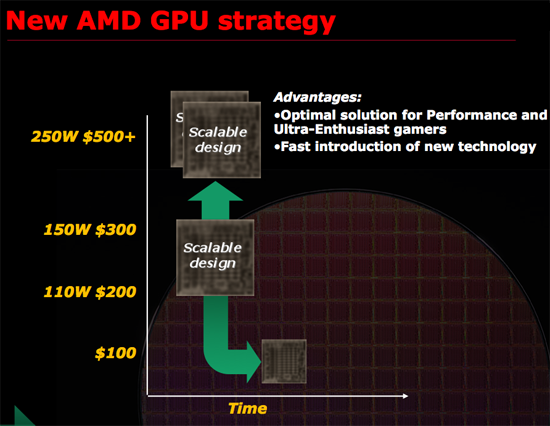
The R700 GPUs introduced AMD/ATI's scalable design process:

amd3.png


They don't need to start with say an rv730 and then adjust it, they can build the chip up with the building blocks they already designed. Remember in that generation the rv770 was originally designed with 640 shaders but they found they could add another couple of shader groups because they had space left over in their design, this was one reason why they caught nVidia off guard.

See here how they scale:

diag_rv730.png


diag_rv710.png


We can see that RV730 differs from RV760 in the number of various execution units: ALU, ROP, TMU. Everything else is the same.

http://ixbtlabs.com/articles3/video/spravka-r7xx-p5.html
 
It'll be awkward when, in 3/4 years, high-end smartphones and mid-end tablets with Android and WP8 come more powerful than the Wii U with about the same autonomy.

Unlike their claims, one can definitely tell that Nintendo's main concern wasn't to spend little power and to create a small console. It was to be greedy and save some $30/unit on sub-par processing hardware.

The idea of the screened controller is spectacular, but it's going to be a dead end as soon as Android/Win8 tablets/smartphones get decent gaming peripherals with Splashtop/Project Glass alternatives. WVGA for a 6" screen, resistive panel against 720p 7" capacitive screens which actually double as tablet computers on the go for about the same price?
Nintendo cheapened out way too much this time. Kicking the sand into the air saying generic stuff like "it's HD" isn't enough.

Precisely, and you have to love how Iwata tries to spin their relentless cost cutting:
Of course, the issue of performance was not secondary. Anyone can realize low performance with low power. Others tend to aim for high performance with high power. With Wii however, Nintendo alone has pursued high performance with low power consumption."

Lol
 
The 40nm eDRAM density is slightly higher than IBMs on 45nm SOI (0.067um2). On IBMs process, that works out to 0.24mm2 finished 1Mbit macros or 32MByte in 61mm2, so the same amount on UX8 might be 55mm2 or so, leaving on the order of 100mm2 for the rest of the GPU if initial size estimates are correct.

For whatever reason, bgassassin seems adamant that the GPU is made using finer lithography. I have no idea what he bases that on.

You probably have no idea what it's based on because I'm not adamant about it. ;)
 
in 3-4 years cell phones and tablets will be on 20nm, I doubt this will allow them to catch up the Wii U and its vastly high power budget. Anyway power isn't everything, Palm Pilot didn't threaten a 1989 Game Boy for gaming, because the Game Boy had gaming controls as standard and a real game library. Good luck getting your phone games planned around using them rather than targetting the 99% touch screen only devices.
 
Precisely, and you have to love how Iwata tries to spin their relentless cost cutting:


Lol

Well if the WiiU allows for better graphics(more powerful) than PS360 while at the same time being smaller and consuming less power,how is Iwata wrong or even spinning?
Considering these statements are all relative.
 
I think this measure has quite a large error.

Total external width for the WiiU is 17.3cm


wii_u_output.jpg


If you look at this picture you see how much room there is on the left side of the power connector and on the right side of the USB-ports. The power connector and USB-ports are at the opposite ends and at the very end of the green usable area of the PCB.

slide008.jpg


I'd say the green area of the PCB can't be much wider than around 13cm and the MCM easily fits more than 3 times on it. Around 3.4 times according to me :) That would make the height of the MCM to be about 37.5mm.

slide003.jpg


I'm sure I have a large margin of error too, but I just can't see the GPU being 280mm2 or even close.
Well I was making you a huge answer because I was wondering how I managed to overshoot it by that much. While doing this I made measurements like you can fit 4 Mcm on the whole mobo, etc. Was considering the spacing between connectors between the first and second pictures of you post to guestimate the size of the mobo. Ultimately I realize that my measurement is fucked up in more than one way as I used the HDMI connector instead of the USB one... :Lol:
Worst part is that it should be wider...

Anyway your measurement is likely to be better. Eye balling tell me that the power plug is ~ 1 hdmi port away from the border of the case. that would put the whole mobo ~15cm and indeed the green part close to thirteen.

I've made an honest mistake, the reference I use was too tiny (and wrong on top of it) to make really accurate measurement on such a low quality picture.

I can live with 37.5x 37.5 which is 1406mm^2 (quiet a difference).
Eye balling of the GPU still works though +/- 9 GPU within the MCM which result into =< 160 mm^2.

That solves the discrepancies I had with the CPU, which might be really tiny (like =< 35mm2).
It discard any significant amount of edram. I still hope Nintendo went along with IBM into a significant rework of say a PPC 470 / to the point it is something new :LOL: that would resemble what I described earlier. Starting from the 4mm^2 ppc476 takes, it could still be doable.

For the GPU well, with more correct data I think that Renesas/NEC 40 nm process might have been used. It was an honest mistake I did not implied that 55nm was used for the sake of making the system looks bad, just for what seems to be the power of the GPU (I would say low clocked RV730/redwood) and wrt size I found 55nm made sense. Anyway from my pov it doesn't change nothing about what the GPU ultimately can achieve.

I'm still willing to learn more about the CPU cores. I'm still a bit underwhelmed by the whole thing as BC seems to be what lead the design choices.
 
Last edited by a moderator:
Well if the WiiU allows for better graphics(more powerful) than PS360 while at the same time being smaller and consuming less power,how is Iwata wrong or even spinning?
Considering these statements are all relative.

Umm... it's coming out 7 years after those machines and it seems to have a weaker CPU than both.
It's like a car manufacturer boasting how its brand new model is way better than competitors from 1992.
Except the new car's engine isn't as good as its 20 year old competitors.

Plus, next year when 720 and PS4 come out, the converse of what Iwata is claiming will be true.
The Wii U will be the one 'realizing low power with low performance'
 
Last edited by a moderator:
Well if the WiiU allows for better graphics(more powerful) than PS360 while at the same time being smaller and consuming less power,how is Iwata wrong or even spinning?
Considering these statements are all relative.
Honestly it is not such an achievement, the lowest GPU AMD cheap is Ciacos. It's not that far behind something like RSX.
But I do agree that he is not lying neither giving things a crazy spin quiet fair.
The WiiU is a real GPU centric design which neither the 360 nor the ps3 were.
 
You probably have no idea what it's based on because I'm not adamant about it. ;)
Did you hear anything new about the amount of on chip memory /edram included in the GPU and the way the GPU access it? (pretty much a confirmation of the 32MB).
With such an amount of Edram and Nintendo giving a bit more details about its design choices, I still wonder why they don't speak of something like free AA which (depending indeed on how the gpu access the on chip memory pool) should be free.
 
Last edited by a moderator:
Hmm, well, that doesn't bode well - especially since it's become quite clear that the CPU is far from the Power7 workhorse, a few were expecting.

It basically seems to be a repeat of the Wii ( where it's better in most areas compared to previous gen consoles but weaker in others.
But that's what most of us were expecting anyway:
http://forum.beyond3d.com/showthread.php?t=61765

I wonder why bgassassin (and a few others) thought it was going to be closer to the next gen machines than the current consoles.
 
Last edited by a moderator:
Anyway your measurement is likely to be better. Eye balling tell me that the power plug is ~ 1 hdmi port away from the border of the case. that would put the whole mobo ~15cm and indeed the green part close to thirteen.

I've made an honest mistake, the reference I use was too tiny (and wrong on top of it) to make really accurate measurement on such a low quality picture.

I can live with 37.5x 37.5 which is 1406mm^2 (quiet a difference).
Eye balling of the GPU still works though +/- 9 GPU within the MCM which result into =< 160 mm^2.

I have to say that I'm still not super confident about my measurements either, so let's just wait and see what the results actually will be :) However I'm thinking that the MCM board actually has an area of about 10.5 times the GPU die, but perhaps the MCM is a bit bigger than 1400mm2. I could see it being 40mm x 40mm = 1600mm2.
 
Did you hear anything new about the amount of on chip memory /edram included in the GPU and the way the GPU access it? (pretty much a confirmation of the 32MB).
With such an amount of Edram and Nintendo giving a bit more details about its design choices, I still wonder why they don't speak of something like free AA which (depending indeed on how the gpu access the on chip memory pool) should be free.

Nothing's changed really. It's 32MB in the Mem1 position. If the eDRAM is used fully as a FB then according to Nintendo it's capable of 4x MSAA with 720p. Not all devs will likely use it as a FB though so that's probably why it's not talked up heavily.

Well, it makes you wonder when you take ERP's little nugget in the other thread ("not even close to 600GFLOPs"). That basically discounts a 640ALU part. ahem

At any rate, I'd hope the clock isn't so low that the triangle throughput is, to be blunt, shit.

I've heard "both ends of the spectrum" so I don't know if we'll ever accurately know. And my take on the final clock has been 480Mhz.

Hmm, well, that doesn't bode well - especially since it's become quite clear that the CPU is far from the Power7 workhorse, a few were expecting.

It basically seems to be a repeat of the Wii ( where it's better in most areas compared to previous gen consoles but weaker in others.
But that's what most of us were expecting anyway:
http://forum.beyond3d.com/showthread.php?t=61765

I wonder why bgassassin (and a few others) thought it was going to be closer to the next gen machines than the current consoles.

Depends on what you mean by "closer". I've said it would be closer in design emphasizing the GPU over the CPU and implementing low power CPUs. I'm on record as saying Wii U is not on par with the other two consoles in graphical power.
 
Will we at least learn final clocks when people hack it and run linux on it or something?

Lol.

I've heard "both ends of the spectrum" so I don't know if we'll ever accurately know. And my take on the final clock has been 480Mhz.

Doesn't fit with Matt's comment though imo. His comment to me reads like 580 mhz or something (totally disregarding any multiplier considerations here, only considering semantics). At least over ~500 mhz.

I have to say that I'm still not super confident about my measurements either, so let's just wait and see what the results actually will be However I'm thinking that the MCM board actually has an area of about 10.5 times the GPU die, but perhaps the MCM is a bit bigger than 1400mm2. I could see it being 40mm x 40mm = 1600mm2.

Seems to me we can take somewhere in the ballpark of 150mm^2 for now. Which is still good work. And a not insignificant chip. Too bad about the tiny CPU.

If you had a 150mm CPU you'd have 300 mm of silicon which isn't terrible compared to PS3 and 360 launch. As is you have maybe 180mm, compounded with it probably being one node higher than Sony/MS will launch at.

It shows a year helping too. 28nm might have been just a tad bit dicey this year for fabbing new designs, but should be good to go by late 2013 without any problems.
 
Status
Not open for further replies.
Back
Top