Why aint X2-Chips looking like this?

Npl

Veteran
attachment.php

I wander why AMD/ATI (or Nvidia for that matter) isnt applying something similar to this - have "X2" dies compromising 2 RV770 cores including interconnects on each waver. If one of em is faulty, simply cut the die in halve and have 1 working core (could also just use the whole die with one core disabled).

The advance would be that there could be a broad bus between both cores, way fatter then whats possible if you use some generic Bus, due to known tracelenghts and no need of solderpads or pins on the packaged chip. À la Cells EIB, only way fatter. Both cores memory-controllers could then more or less use the full bandwidth of all connected memory-modules.
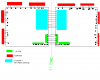
In the pic above I also linked the half of the PCIe-lanes together, in the case of a damaged core, the traces will again be cut and the solderpoints used. This should allow them to get rid of additional PCIe-bridge chips rather easy.. and additional bandwidth if BFI aint enough

Advantages (for full X2-dies):
  • less Pads/Pins than 2 individual packages
  • also less lanes on the PCB and possibly less layers because of that
  • BFI (big fat interconnect) - short, simple and fat bus between cores. If you match the bandwith to be 2x the membandwith of 1 core, then you practically have a 512bit bus that either one core can exploit alone (with some added latency if its going thru the other core - but latency aint an issue for GPUS) or dynamically share. No need for seperate banks anymore
  • With a bit of replication and sorting of signals theres no need for an PCIe-Bridgechip.
Disadvantages:
  • unused traces and buses from the memory-controller on single cores.
  • some unused logic on the PCIe controller
  • possibly problems in the production-pipeline if cuts are conditionally?
 

Attachments

  • GPUX2.PNG
    GPUX2.PNG
    13.9 KB · Views: 476
If one of em is faulty, simply cut the die in halve and have 1 working core (could also just use the whole die with one core disabled).
You can't conditionally cut a die. Wafers are diced with circular saw that go through the whole wafer.
 
Technically this is already done on a lot of not-quite-high-end chips (and some low-end chips too, I thnk) already. A chip could have 8 parallel elements to it, but if tehre's an error in one of those elements on a chip, the company will just zap that part out so that it's disabled. That chip is now the same as a low-end version of the same chip. AMD and NV have done it with their chips for a long time, and typically the chip just below the high end is a victim of this, e.g. the 8800 GTS compared to the 8800 GTX. It's not necessarily GPU exclusive either, as IBM's Cell chip is the same way, and I'm sure if you looked around, you'd find examples of it in intel and AMD's lineup.
 
correct, this sort of disabling of chip elements is prevalent.

its not only for parts with errors, parts that dont speed bin out at the top also get elements disabled and then get sold as the lesser part.

this has been a practice since at least the R300, this page
http://www.hardwaresecrets.com/article/49

talks about a hardware mod to convert a 9500 to a 9700, the 9550 moved this "loose end" completely on die so this sort of creative mod'ing was no longer possible.
 
PhilTaylor: hang on, no need to repost as the first few posts are moderated and must be aproved.
 
I allways wondered why x2 gpu's were'nt like this:


with the second gpu not being a full gpu just containing what a normal gpu has multiple's of
 
The original post's scheme has a few other things that might be "different", if not more difficult, for a high-volume design.

The two cores are not exact duplicates, but mirror one another.
It's perfectly doable, though it may turn out that the fab will be using a mask that has a double-wide chip with two mirrored halves, rather than trying to fiddle with exposing a single core twice with a flip. I don't know enough about fabbing to say what exactly can happen.

Low volume runs with small clients can have different chips put on the same wafer at a foundry, but that's on a very different scale compared to a mass-produced product, and I don't know if the foundry just partitions the wafer with coarsely sized individual regions getting the same kind of chip, rather than every other chip being different.

Intel has had products where single cores are cut from a wafer in pairs.
Some large CMOS chips are made of many smaller chips that are stitched together at the wafer level if the overall product is too big for the reticle size.

I don't know about combining both approaches, though I suppose it is at least physically possible. Doing this has been talked about before in this forum.

As for conditionally cutting, this is not likely to happen.
Aside from obvious physical defects, the die needs to be mounted and packaged for full verification, in which case it is too late to cut one off.
Even in the case of defects seen on the wafer, the effort to shift around cuts in a running production line might incur costs exceeding the saved dies, or is simply not practical with standard wafer cutting tools.
More likely, it's a case of cutting out pairs and hoping for the best.
 
The original post's scheme has a few other things that might be "different", if not more difficult, for a high-volume design.
Yeah, he was not talking about disabling individual parts, but about cutting different sized dies out of a wafer depending on defects or required volume.

The two cores are not exact duplicates, but mirror one another.
It's perfectly doable, though it may turn out that the fab will be using a mask that has a double-wide chip with two mirrored halves, rather than trying to fiddle with exposing a single core twice with a flip. I don't know enough about fabbing to say what exactly can happen.
You can't mirror a single mask. As you suspected: it's a little more complex than the negative of a 35mm camera. ;)
But nothing prevents you from putting multiple dies on a single mask. In fact, for smaller dies, that's exactly what happens. If your mask covers 25x25mm and your die is 10x10mm, it's standard practise to put 4 copies on a single mask. This way, the speed of exposing a wafer is less dependents on the size of the die.

Low volume runs with small clients can have different chips put on the same wafer at a foundry, but that's on a very different scale compared to a mass-produced product, and I don't know if the foundry just partitions the wafer with coarsely sized individual regions getting the same kind of chip, rather than every other chip being different.
For a multi project wafer, each wafer will typically result in 1 type of chip, the rest of the silicon is scrap. So if you have 5 different chips on a mask, you need to run at least 5 wafers to get samples of each of them.

... or is simply not practical with standard wafer cutting tools.
It's basically not possible. Like cutting out individual square out of a wooden plank with a circular chain saw.
 
I know about disabling titles, but obviously AMD did choose to produce smaller cores instead of big monolithic ones (AMDs topend is 2 GPUs on 1 Card, Nvidia has big monolithic cores). So the idea is basically to create "smaller" cores, but to have them already connected on the wafer.
I know there are probably alot of practical reasons against this, but Im curious what those reasons are.


It's basically not possible. Like cutting out individual square out of a wooden plank with a circular chain saw.
Its not like you cut out singular dies by themself. Even with regular dies you have to do a horizontal and vertical "pass" with the saw. I dont think it would be problematic to cut a row of chips (after first pass) and make additional cuts if necessary. Certainly wont be a problem with wooden planks (I can relate to this more than fabbing ICs;))


As for conditionally cutting, this is not likely to happen.
Aside from obvious physical defects, the die needs to be mounted and packaged for full verification, in which case it is too late to cut one off.
Even in the case of defects seen on the wafer, the effort to shift around cuts in a running production line might incur costs exceeding the saved dies, or is simply not practical with standard wafer cutting tools.
More likely, it's a case of cutting out pairs and hoping for the best.
Hmm, I feared this would pose big problems in the workflow. Thanks.
 
Its not like you cut out singular dies by themself. Even with regular dies you have to do a horizontal and vertical "pass" with the saw. I dont think it would be problematic to cut a row of chips (after first pass) and make additional cuts if necessary. Certainly wont be a problem with wooden planks (I can relate to this more than fabbing ICs;))
You could do an additional cut, but it would have to be all or nothing: cut all the dies along a vertical or horizontal line in two or not... That may or be good enough in some cases, but it's definitely outside the regular production flow.
 
I allways wondered why x2 gpu's were'nt like this:


with the second gpu not being a full gpu just containing what a normal gpu has multiple's of

expanding further.. wouldn't it be nice if you had 1master gpu with control logic, some shaders and rops, and a lot of sockets on the PCB to add dies with a MC and math area? say 1 central GPU with 200SP,10TMU 16ROPS, and 1-4(8?) sockets for 400SP/20TMU units...for starters
Code:
0      0     0
   m     m
0-m-M-m-0
   m     m
0     0      0
 
Back
Top