The Official RV630/RV610 Rumours & Speculation Thread

Status
Not open for further replies.
aopen-5900xt-scan-front-small.jpg

gffx5800u-scan-front-small.jpg


One of the above cards has a 256-bit bus. The other one has a 128-bit bus. Both have 128MB of RAM. Using you bus width-to-PCB length correlation formula, would you please tell me which one is which?

5800xt have 256bit the 5800ultra have 128bit, still no one of this pcb longer than 20cm, and this cards maked years ago ;)

I not say the long PCB equal the 256bit, but the chance its a 128bit card is very low this days.
 
Can anyone explain what exactly is calculated by a texture addressing unit?
The addressing unit takes the texture coordinates of a quad as input, as well as their pos.w value for perspective correction, I believe. Based on that, it determines what samples need to be fetched and what their weights are.
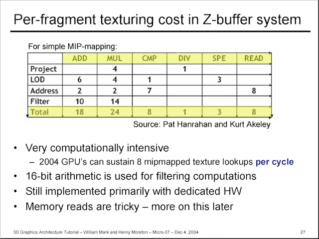
So, that's mostly control logic, while filtering is mostly computation. These are ALUs, not FPUs, though; at least on G7x. The exponent for a block of bilinearly filtered pixels is shared when filtering.

I've already said this before, but that might be another reason why 'free' 2x filtering might make sense because it looks to me like a very logical part of the pipeline to implement in custom (semi- or full) logic and just double-pump. I don't know if that's actually the case on the G80, but it wouldn't surprise me.

Another reason why it made sense to me on G80's launch that addressing power was lower is that it might become a much more expensive part of the texturing process with AF quality as high as on the G80's. However, given that the G84/G86 now have a 1:1 ratio again, I'm not so sure. It will be very interesting to see what the 65nm iterations of the architecture look like, I think... :)
 
The funny thing is that the RV630XT has a power consumption of 128W, while the 8600GTS is numbered 47W according to xbitlabs.

Ones dual slot, and much longer than the 8600GTS.

The RV630XT could be in a whole new different league, and may well perform close to the 8800GTS 320 ballpark by the looks of things.
 
The addressing unit takes the texture coordinates of a quad as input, as well as their pos.w value for perspective correction, I believe. Based on that, it determines what samples need to be fetched and what their weights are.

Ah, I didn't realize it also still had to do perspective correction. So that's basically a division operation, right?

One more question: I can see that it makes sense to operation on a quad in a R580 or G71 design. But is that still true for an R580 or a G80 architecture? If you have divergent branches in your shader program, different pixels of a quad may have radically different texture needs, right? Or will they, upon the request for the first pixel, fetch the texels that are assumed to be required for all pixels assuming some gradual transition and store them in the cache until later pixels do their request?

Thanks!

Edit: more than once, I've thought it would be very useful to have a reference article that goes through the GPU pipeline and spells out the individual steps in a mathematical and algorithmic way that gives a detailed insight into how much data/samples/attributes go in, what is calculated, and what goes out.
 
Last edited by a moderator:
just about to say that myself, whats going on with these midrange cards? no one whats the market for themselves ! :D
 
Interestingly, RV530 was deployed in two GPUs, X1600XT and Pro with bandwidth of 22.1 and 10.9GB/s. So, in a sense, there's a precedent for a 2:1 ratio in bandwidth based on the "pro" board. But X1600XT was blessed with considerably more bandwidth than was useful - X1650XT, with twice the ALUs, TMUs and ROPs is upto 75% faster (typically 35%) with slightly less bandwidth than X1600XT.

That score of 2105 in 3DMk06 SM3 test is pretty much the same as a stock 8600GTS, e.g. 2029:

http://www.xbitlabs.com/articles/video/display/geforce8600gts_21.html

Jawed
 
According to the author, it is saiid that the board uses 256MB of GDDR4. The 65nm manufacturing process GPU comes with a BIOS dated Apr 4th. Max wattage is 80W or lower. There is no additional power connector unlike the NVIDIA 8600GTS. In one of the 1080P video tests, cpu utilisation is lower than 5% on the average. That is amazing.
Link

Looks like the rv630xt 256mb gddr4 121watt TDP was a FUD.
 
Nice to see a single slot cooler. Lets hope it's not a 2400 card on that pic. :smile:
But if the 2600XT doesn't require a power connector I'm really impressed.

And you can't go wrong with flames. ;)
 
I realised just now those flames are supposed to be ice expanding across the cooler :LOL: :LOL: :LOL: guess the graphical concept needs a rethink.

Hmm, the power is down, but 80W would still require extra power, wouldn't it? Unless the person saying 80W is guesstimating from measurements at the wall or something.

Looking at the picture, there's a capacitor in the top right corner, right on top of the set of 6 holes for the PEG power connector. So, that board definitely doesn't have extra power.

I assumed this was a lower spec board when I examined it last night. If it's GDDR4, then maybe not. Is the 512MB GDDR4 version the only one requiring extra power?

Jawed
 
I read somewhere that Ati targeted RV630 to be "faster than X1950GT", don't remember where it was or which RV630, but it sounds to be vey much like 8600GTS.
 
Hmm, the power is down, but 80W would still require extra power, wouldn't it? Unless the person saying 80W is guesstimating from measurements at the wall or something.
The PCI-SIG won't validate it if it honestly could ask for > 75W from the slot at any time. So you're probably right.

As for a 512MiB GDDR4 variant requiring more power (and one would assume that configuration of RV630 would be an XT of some kind), I'd say so. But don't think that dual-slot version seen previously is such a config.

I'd note that the dual-slot version and this one we're seeing now look to have the same (or very similar) PCBs, too. That's somewhat telling.
 
Status
Not open for further replies.
Back
Top