Samsung Exynos 5250 - production starting in Q2 2012

  • Thread starter Deleted member 13524
  • Start date
Okay, that's a good point and explains the Chromebook's load consumption, but I'm still not convinced that A15 is much better than Clovertrail under a ~2W SoC thermal envelope.

But you say this without knowing either what Clovertrail or Exynos 5210 (nevermind Cortex-A15 on other SoCs) can sustain while under a 2W limit.

Look at the power curve in Nebuchadnezzar gave for the 32nm Exynos 4, and how it really starts gaining tremendously past 800MHz. What if Exynos 5 uses half as much power at peak while at 1.4GHz? What if it uses a third as much at 1GHz? We don't know what its curve is like (where the knee is).

We also don't really know what the OS conditions were like for the the Chromebook test. Saying that ChromeOS has great power tuning because it's done by Google is naive; it's a tweaked Gentoo Linux with Chrome on top. When I run Kraken on my Mint desktop I see the active (100% utilization) thread rapidly (as in, several times a second) moving between CPU cores. This isn't a good scenario for minimizing power consumption. Some usage graphs would be helpful. Does anyone know if Exynos 5 has separate clock/voltage planes for the two cores?
 
But you say this without knowing either what Clovertrail or Exynos 5210 (nevermind Cortex-A15 on other SoCs) can sustain while under a 2W limit.

Look at the power curve in Nebuchadnezzar gave for the 32nm Exynos 4, and how it really starts gaining tremendously past 800MHz. What if Exynos 5 uses half as much power at peak while at 1.4GHz? What if it uses a third as much at 1GHz? We don't know what its curve is like (where the knee is).
That curve is for 45nm. I thought I put enough emphasis on that. The 32nm versions is really about exactly what Samsung claims it to be, little bit more than half on the same frequency and core count.

It doesn't. They are still on a single frequency plane for all the cores. Core independent clock-gating idle state, and CPU-wide power collapse idle state (While running).
 
Last edited by a moderator:
That curve is for 45nm. I thought I put enough emphasis on that. The 32nm versions is really about exactly what Samsung claims it to be, little bit more than half on the same frequency and core count.

You did put enough emphasis on that. I'm using that curve as an example that power consumption isn't linear with frequency, not as a direct representation of how Exynos 5 consumes power (and I wasn't talking about the 32nm Exynos 4). Not linear puts a greater emphasis on the fact that we don't know where the "knee" of the curve is. We don't know what the currently available Exynos 5s can clock to while staying within a 2W envelope (if they wanted to for whatever reason)

I don't remember Samsung claiming that 32nm has half the power consumption for the same 45nm designs, though. I remember something like 40% less active power.

It doesn't. They are still on a single frequency plane for all the cores. Core independent clock-gating idle state, and CPU-wide power collapse idle state (While running).

That sucks. Is this a limitation in Cortex-A15 itself? Does Atom not have this problem? I imagine no one would know if Swift does..

It's a moderate problem for 2 cores and a pretty substantial one for 4 cores.

Note that in this case it means if the OS wants to schedule any activity for the other core at all it needs to keep it at full clocks, and if there's lots of intermittent (but not steady) activity spikes that it doesn't want to interrupt a full load core with it could mean you're seeing much higher power consumption than you would if that workload were done on one core only.
 
Solid scores for the T-604 but 554mp4 is in a different league entirely.

Looking forward, the Mali roadmap doesn’t look terribly promising either. The best they have to offer is the t678 in mp8 configuration. That will have 4x the gflops of t604(at the same clocks) but texture throughput, pixel fillrate etc. will only get doubled, which is worrying because PowerVR is already there on those metrics.
It seems to me they are focussing too much on shader performance when a more balanced approach would have been better. They will really struggle against rogue..

Anyone else share the same concerns?

Share the same concerns yes, I just disagree that Mali T6xx concentrates too much on shader peformance. It's rather the exact opposite. The Mali T604 clocks at 533MHz and has a theoretical peak of 72 GFLOPs from its ALUs. The SGX554MP4 in A6X on the other hand should clock at 280MHz with a theoretical peak of over 80 GFLOPs; clock the latter at 533MHz and the comparison gets even more colourful.

With Rogue the FLOP-saga gets times worse since the GC6400 4 cluster Rogue GPU is according to IMG exceeding the 200 GFLOPs mark; that always on a MP4 or 4 cluster comparison. In fact it might have been a better idea for ARM to focus more on FP32 floating point throughput and skip native FP64 hw support. Always IMHO.
 
You did put enough emphasis on that. I'm using that curve as an example that power consumption isn't linear with frequency, not as a direct representation of how Exynos 5 consumes power (and I wasn't talking about the 32nm Exynos 4). Not linear puts a greater emphasis on the fact that we don't know where the "knee" of the curve is. We don't know what the currently available Exynos 5s can clock to while staying within a 2W envelope (if they wanted to for whatever reason)

I don't remember Samsung claiming that 32nm has half the power consumption for the same 45nm designs, though. I remember something like 40% less active power.
The 40% figure came from the 4212 which never saw the light of day in any device; 1.4GHz vs 1.2GHz 4210 and higher clocked Mali resulted in 40% less power in the end. Samsung claims 20% less power on the 4412 over the 4210 with double the core count and higher clocked Mali. I find their claims to be pretty accurate, even though I haven't measured it empirically.
That sucks. Is this a limitation in Cortex-A15 itself? Does Atom not have this problem? I imagine no one would know if Swift does..
It's a limitation of the power management IC and SoC design, you would have to have as many power rails as CPU cores to have fully independent DVFS on the SoC. The core architecture doesn't really come into play here at all. Here is a in-depth paper of the problems and solutions: http://www.cs.utah.edu/hpca08/papers/1B_4_Kim.pdf

Qualcomm claims separate power planes but I'm more of the Samsung expert and don't know what and how they do it (Heck, even Samsung's JK Shin head of mobile claimed it for the 4412 but there's absolutely no sign of it in either reality or even SoC manuals).
 
Share the same concerns yes, I just disagree that Mali T6xx concentrates too much on shader peformance. It's rather the exact opposite. The Mali T604 clocks at 533MHz and has a theoretical peak of 72 GFLOPs from its ALUs. The SGX554MP4 in A6X on the other hand should clock at 280MHz with a theoretical peak of over 80 GFLOPs; clock the latter at 533MHz and the comparison gets even more colourful.

With Rogue the FLOP-saga gets times worse since the GC6400 4 cluster Rogue GPU is according to IMG exceeding the 200 GFLOPs mark; that always on a MP4 or 4 cluster comparison. In fact it might have been a better idea for ARM to focus more on FP32 floating point throughput and skip native FP64 hw support. Always IMHO.

Hmmmm, taking clock speeds into account it seems 554mp4 and t604 are very similar in terms ALU performance ( ~70 gflops) and texture throughput (4 tmus at ~500mhz vs 8 tmus at ~250mhz).

What exactly is holding the t604 performance back? Is it bad drivers? is TBDR that much of an advantage?
 
Hmmmm, taking clock speeds into account it seems 554mp4 and t604 are very similar in terms ALU performance ( ~70 gflops) and texture throughput (4 tmus at ~500mhz vs 8 tmus at ~250mhz).

What exactly is holding the t604 performance back? Is it bad drivers? is TBDR that much of an advantage?

Could very well be an unoptimised compiler and/or driver. It might be complete bullshit but ARM just started with T604 using USC ALUs for the first time. If there's something driver related at play we should of course expect things to get better as time goes by.

Or the rasterizer/trisetup is too weak on T604 and is holding it back, since it's geometry scores are relatively low too. Remember the MP4 consists of 4 cores and it has one raster/trisetup unit per core.
 
Share the same concerns yes, I just disagree that Mali T6xx concentrates too much on shader peformance. It's rather the exact opposite. The Mali T604 clocks at 533MHz and has a theoretical peak of 72 GFLOPs from its ALUs. The SGX554MP4 in A6X on the other hand should clock at 280MHz with a theoretical peak of over 80 GFLOPs; clock the latter at 533MHz and the comparison gets even more colourful.

With Rogue the FLOP-saga gets times worse since the GC6400 4 cluster Rogue GPU is according to IMG exceeding the 200 GFLOPs mark; that always on a MP4 or 4 cluster comparison. In fact it might have been a better idea for ARM to focus more on FP32 floating point throughput and skip native FP64 hw support. Always IMHO.

I am concerned that the parties involved in mobile GPUs are putting out BS numbers for flops. And it's not just a matter of the numbers being useless.

When nvidia/amd put out Tflop numbers, you can atleast see how they got there architecturally. Obviously those numbers have a tenuous correlation with actual performance at best, but the raw numbers per se are solid.

In mobile, there is ZERO architectural disclosure. I am concerned that those numbers are BS to begin with.

Fortunately, OpenCL ES should debut soon, which will help clear the matters.
 
For IMG, the programmable flops numbers are correct.

9 flops per USSE2 (vec4 MAD + another dual issue flop), 8 per 554, 4 of them in SGX554MP4, so 288 flops per clock there.
 
I am concerned that the parties involved in mobile GPUs are putting out BS numbers for flops. And it's not just a matter of the numbers being useless.

When nvidia/amd put out Tflop numbers, you can atleast see how they got there architecturally. Obviously those numbers have a tenuous correlation with actual performance at best, but the raw numbers per se are solid.

The latter goes for the desktop albeit not really always either: http://www.beyond3d.com/content/reviews/1/11

AMD is currently absent from the small form factor market, while NVIDIA has its presence with Tegra.
In mobile, there is ZERO architectural disclosure. I am concerned that those numbers are BS to begin with.

Fortunately, OpenCL ES should debut soon, which will help clear the matters.

That goes for all involved parties more or less, NVIDIA/Tegra not excluded. In fact they've got more to hide than to market up to now especially when it comes to GPUs. The ULP GF in T3 has "12 cores" and that's all you need to know. They haven't even disclosed any theoretical fillrates so far, meaning that there's a whole damn lot of guesswork surrounding the actual architecture. And not they're of course not the only ones. It's an annoying general trend with varying degrees between GPU vendors.
 
It's a limitation of the power management IC and SoC design, you would have to have as many power rails as CPU cores to have fully independent DVFS on the SoC. The core architecture doesn't really come into play here at all. Here is a in-depth paper of the problems and solutions: http://www.cs.utah.edu/hpca08/papers/1B_4_Kim.pdf

Qualcomm claims separate power planes but I'm more of the Samsung expert and don't know what and how they do it (Heck, even Samsung's JK Shin head of mobile claimed it for the 4412 but there's absolutely no sign of it in either reality or even SoC manuals).

But the core architecture does come into play, because you don't just place separate Cortex-A15 cores down on the SoC and clock them as you please; when you license the IP you're configuring multiple cores with a shared L2 cache and possibly other communication pathways between them. So the Cortex-A15 design itself needs to be capable of asynchronous clocking and I'm asking you whether or not it is, so I know whether or not it's even possible that future SoCs are asynchronous. If it supports it obviously the rest of the SoC and PMIC have to accommodate the separate clock/power domains, that was never under question.

I was under the impression that it was not possible with Cortex-A9, and I was hoping this wouldn't be a disadvantage for every Cortex-A15 SoC. At least big.LITTLE would have to have separate domains for the big and little clusters. You can also pair two separate Cortex-A15 clusters so this could be another way to (presumably) get asynchronous domains if it isn't possible otherwise.
You're asking me the wrong questions then, I can answer more or less specific platform questions, for architectural things you need to refer to somebody else. If it is an architectural limitation then Qualcomm is enjoying a rather big power management advantage ever since their Scorpion cores, which hasn't got any publicity at all as a feature. This also makes JK Shin an even bigger idiot for making those claims back in May. I do wonder what the real benefits of it would be in contrast to the fine-grained clock gating that does take place right now. I gather that ARM would address it by now if it did bring an easy power improvement.
 
The GLBench listing for the Nexus 10 shows that its drivers/software are shipping in basically the same state for performance as the Arndale board which just preceded it, other than v-sync and dvfs being apparently off for the dev board's single bench run (and the first run through the benchmark's "game" tests do tend to understate overall performance by several percent.)
 
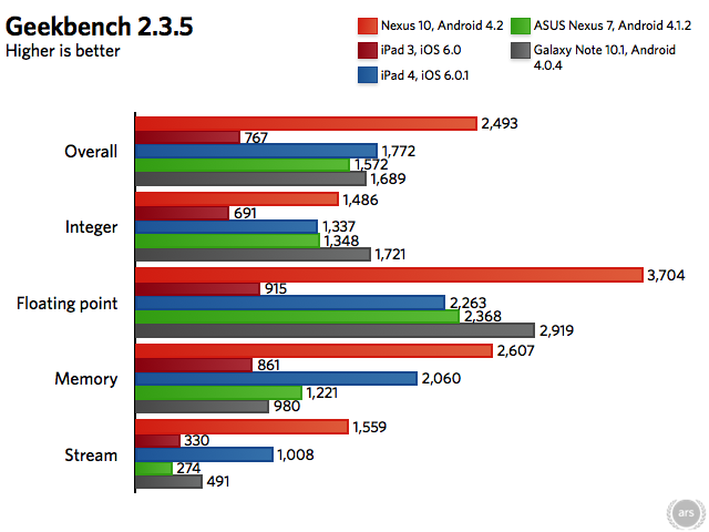
ArsTechnica has a review up with some benchmarks; notably most new is the Geekbench one:

Nexus-10-charts.005.png


Impressive memory scores compared to the A9's and even Swift, but then again, it has double the bandwidth available compared to all the others in the chart.
 
Last edited by a moderator:
Read more at EETimes.
Samsung will detail a 28-nm SoC with two quad-core clusters. One cluster runs at 1. 8 GHz, has a 2 MByte L2 cache and is geared for high performance apps; the other runs at 1.2 GHz and is tuned for energy efficiency.

The chip coincides in some specs with the 5450, but they well may be two different entities, however the timing between the two is far too close in my opinion to warrant their co-existence.
 
Last edited by a moderator:
I always thought that the 5250 would end up in phones and the 5450 would be in tablets. Perhaps they'll be reversed to compete with the Tegra 4?
If it's a big.LITTLE implementation then the form factor is irrelevant, they can still go full-fledged quad as the A7 cores will allow for the power efficiency.

Several hours ago Samsung uploaded a patch support for a 5440 on the Linux patchwork: https://patchwork.kernel.org/patch/1653051/

This is the first mention of that codename. We might well have two different quads coming.
 
Don't know why I didn't do this sooner, but a quick look on the Cortex-A15 TRM shows that it doesn't support asynchronous clocks for different cores:

http://infocenter.arm.com/help/index.jsp?topic=/com.arm.doc.ddi0438e/CJHFFIHH.html

Samsung actually released a paper quite a while ago arguing for big.LITTLE as an alternative to asynchronous clocking over similar core clusters. http://www.samsung.com/global/business/semiconductor/minisite/Exynos/data/benefits.pdf Some of the arguments don't seem that great, but they do point out that asynchronous domains results in higher latency communication.

I can see a lot of scenarios where you want to use the A7 cores with just one A15 core active, both running at different clocks/voltages.

That's a pretty big advantage for Krait, which is why the S4 doesn't have to waste die space on other lower power cores.
 
That's a pretty big advantage for Krait, which is why the S4 doesn't have to waste die space on other lower power cores.

http://www.samsung.com/global/business/semiconductor/minisite/Exynos/data/benefits.pdf

In Samsung's big.LITTLE whitepaper they actually argue in depth that asynchronous clock architectures bring a big latency disadvantage and thus performance impact. You can argue if the real-world advantage is really that great then.

___


http://www.phoronix.com/scan.php?page=article&item=samsung_exynos5_dual&num=1

Phoronix did some low level Linux desktop grade benchmarks on a Chromebook running Ubuntu, it includes comparisons against Tegra 3, various Atom cores, and a low-power i3. The Exynos beats all the mobile chips handily in terms of CPU performance and holds up its own against the i3, considering its power envelope difference.

___


Furthermore during my kernel hackings, I wondered what a dedicated memory space "srp" stood for in the 4412. I researched a bit and it raised a few eyebrows: Samsung Reconfigurable Processor

http://web.yonsei.ac.kr/wjlee/document/HPG2011.samsung.wjlee.paper.pdf
http://www.highperformancegraphics.org/media/Posters/HPG2012_Posters_W-J.Lee.pdf

The 4210 and 4412 (And 5250 presumably) ship with an SRP based audio "unit".

Can somebody explain what the point of this is? Are they trying to make their own GPU, or is this a research-only FPGA-like test-bed?

___


http://www.koreatimes.co.kr/www/news/tech/2012/12/419_127247.html

The internet rumor mill has been very active on the 5440: Korea Times reports they will have a 4+4 big.LITTLE implementation ready for the Galaxy S4. There has been little doubt that Samsung will be the first to introduce this, but it is big news if they do make it in time for next summer.
 
Back
Top