NVIDIA Tegra Architecture

Seems to be implying that nVidia will be using the same core muxing strategy they used on Tegra 3 but with Cortex-A15s. If that's really what it means then I don't buy it. It works on Tegra 3 because the L2 cache is decoupled from the cores. That's no longer true with A15, so a "companion core" would be a heavy modification of what ARM's offering, and I doubt they're interested in providing such a thing instead of big.LITTLE.

Did Tegra 3's companion core share the L2 with the main cores? I thought otherwise.

Five A15s would also put them at a big die area disadvantage vs dual A15 SoCs, either in having much less to spend on other things like the GPU or IMC, going with low cache values (I can see it now, 4 cores sharing 1MB of L2 cache again..), or offering much bigger dies. Across their entire A15 product offerings, apparently.

Impracticality for marketing sake isn't new....

I also wonder where that third option (screen size?) even fits into this. Are none of these products supposed to be meant for phones at all?

I believe Grey is set to take over the reigns of smartphones.
 
Why 5 A15's?? I would think 4+1 would be four A15's and one A7?? i thought Tegra 3 was a trial run for that architecture?

Because that's how Tegra 3 works. Its companion core is not a "trial run" for big.LITTLE, they're very different technologies. The approach in Tegra 3 doesn't work so well if the processors don't have the exact same external interfaces, which I doubt is true for Cortex-A7 vs Cortex-A15.

It could be that nVidia really is reusing "4+1" to mean four A15 and one A7 with big.LITTLE, but it'd be strange because big.LITTLE at a hardware level doesn't prevent you from running all the cores simultaneously. The exclusivity/core switching part is accomplished in software.

I thought L2 was decoupled from All new arm cores? Don't forget its also on 28nm which will help matters..

No, it's only decoupled in Cortex-A9. Not in A7 or A15, and it wasn't in A8 for that matter. And it wasn't in Scorpion and I can't see why it would be in Krait. Decoupling the L2 gives you more design flexibility but it's worse for performance and it's probably worse for area and power.

Yes, nVidia's next product will be 28nm, but so will everyone else's SoC and they're mainly featuring 2 Cortex-A15s. I bet the increase in area from Cortex-A9 to Cortex-A15 outweighs the increase in density from 40nm to 28nm. But I'm not putting it past nVidia to badly balance this.

metafor said:
Did Tegra 3's companion core share the L2 with the main cores? I thought otherwise.

Read the whitepaper: http://www.nvidia.com/content/PDF/tegra_white_papers/tegra-whitepaper-0911b.pdf It's shared.

But really, you thought that the companion core has its own separate 1MB L2 cache + L2 controller? What advantage would this have provided? You'd probably have to flush the entire cache on a switch too..

metafor said:
Impracticality for marketing sake isn't new....

Yeah, but with Tegra 3 they didn't pay a very big price for their core count, area wise..

metafor said:
I believe Grey is set to take over the reigns of smartphones.

Okay, but what indication do we have exactly of what Grey would include? If SP3X on this list is supposed to be Grey then it's coming out way later than it's supposed to (according to nVidia as of last month, Q4 2012 or Q1 2013)
 
Few thoughts on the leaked 'roadmap':
1) It looks like nvidia keeps their current policy regarding release cycles for their specific SoC's - first standards version, then faster version and after that we get one for smartphones. Wonder how they didn't learn already that they should equally prioritize smartphone and tablet markets, and not focus solely on tablets
2) something new here is SoC with integrated connectivity(could it be Grey?), probably to fight Qualcomm but I fear it'll be outperformed by wide range of Krait powered SoC's from QCOM.
3) if those dates indicate devices shipped to end users it's not that bad, but I fear that they will get postponed as they always do. So 2Q is getting more realistic for market release with huge shows promoting new devices at CES and MWC'2013.

If it's recent, and dates are correct, then I would say that they could be slightly late to the game, and without some kind of out-of-this-world GPU they could lose the battle to TI, QCOM and Samsung. Especially if we consider that later this year QCOM will release msm8960 pro with adreno320(said to be at least 3x faster than current 225), samsung is going to release their exynos 5xxx and we can't forget about TI's OMAP5.
 
Because that's how Tegra 3 works. Its companion core is not a "trial run" for big.LITTLE, they're very different technologies. The approach in Tegra 3 doesn't work so well if the processors don't have the exact same external interfaces, which I doubt is true for Cortex-A7 vs Cortex-A15.

It could be that nVidia really is reusing "4+1" to mean four A15 and one A7 with big.LITTLE, but it'd be strange because big.LITTLE at a hardware level doesn't prevent you from running all the cores simultaneously. The exclusivity/core switching part is accomplished in software.

No, it's only decoupled in Cortex-A9. Not in A7 or A15, and it wasn't in A8 for that matter. And it wasn't in Scorpion and I can't see why it would be in Krait. Decoupling the L2 gives you more design flexibility but it's worse for performance and it's probably worse for area and power.

Yes, nVidia's next product will be 28nm, but so will everyone else's SoC and they're mainly featuring 2 Cortex-A15s. I bet the increase in area from Cortex-A9 to Cortex-A15 outweighs the increase in density from 40nm to 28nm. But I'm not putting it past nVidia to badly balance this.
Different technologies i see.. well if they are keeping the same 4+1 design, and Cortex A7 can't be used...(i still don't see why they couldn't..and just give the A7 its own cache?)..then they certainly wont get the full benefit using an A15...so they would probably reuse the A9?...

I think im getting mixed up with the power gated L2 from krait/Saltwell/A9?...decoupling L2 is a different method entirely?...

Either way, Tegra 4 is going to be the leader if it uses Kepler derived GPU..as they will provide software that utilises it.
 
Either way, Tegra 4 is going to be the leader if it uses Kepler derived GPU..as they will provide software that utilises it.

IF is the keyword here ;)
I don't see how they could use Kepler in tegra4 considering that most design work has been probably finished at this point. And I don't think they decided to use unproven piece of technology in something that is so much important to them.
IMO Kepler will be used with Project Denver CPU. Two of their best engineering achievements to give us highest performance(that is me thinking what will nvidia say to us ;-)).
 
Different technologies i see.. well if they are keeping the same 4+1 design, and Cortex A7 can't be used...(i still don't see why they couldn't..and just give the A7 its own cache?)..then they certainly wont get the full benefit using an A15...so they would probably reuse the A9?...

I'm saying if they do the same thing they did in Tegra 3 they'd need to use an additional Cortex-A15, not that A7 doesn't work but A9 somehow does. A9 would in fact be more problematic because it doesn't have all of the instructions A15 and A7 has.

The point of the matter isn't about whether or not they can pair a single Cortex-A7 with a Cortex-A15 4-core cluster, obviously they can since the coherency protocol allows it and ARM themselves uses it for big.LITTLE (no idea if ARM will let you configure something like 4 A15s with 1 A7 though).

What I'm saying is they can't do the SAME thing they did in Tegra 3. Doesn't actually matter if they use a Cortex-A15 as the companion core, they can't mux one away from the L2 cache. So when I see "4 + 1" I think one of two possibilities:

1) nVidia is capitalizing on keeping terminology consistent even though the approach isn't (and may well not be limited to 4 vs 1 instead of 5 concurrent cores - no reason for this!)
2) The leak, like so many before it, is made up and the author thinks that the same approach as in Tegra 3 can be used because they don't understand the technology

Note the key point here for "the way nVidia does it" is that it's handled completely transparently in hardware. big.LITTLE requires OS support. In order to do this in Tegra 3 they'd have to have to duplicate the same sized L2 cache for that single Cortex-A15 vs the four core one which would be a massive waste.

I think im getting mixed up with the power gated L2 from krait/Saltwell/A9?...decoupling L2 is a different method entirely?...

I'm not talking about separate power rails.

When you buy a Cortex-A9 from ARM it doesn't come with L2 cache. It comes with the usual AXI bus interface, and you have to put a separate L2 cache (including controller) on the other side of this bus. They added a couple of things to the bus as optional cache optimizations, but they warn that it breaks the standard bus operation.

Doing it this way makes the L2 higher latency and quite likely, lower bandwidth, depending on clocking. Usually the core includes L2, and the L2's design is closely integrated into the critical path/pipeline of the processor.

Decoupled L2 means you can interface things besides CPU cores to the same L2. It also means you can do stuff like what nVidia did with the companion core. With tightly integrated L2 you can't do these things the same way.

Either way, Tegra 4 is going to be the leader if it uses Kepler derived GPU..as they will provide software that utilises it.

What makes you so sure about that? I'll entertain the notion that GPU dominance = SoC dominance (I don't believe it at all). But just because Kepler is doing very well in the high end 200+ TDP and perhaps down to the 20+ or so TDP segments, it doesn't mean it'll easily beat other mobile solutions assuming it can really scale down to < 2W in the first place. It still doesn't have the bandwidth enhancements that say, TBDR and PVRTC 2bpp give IMG's Series 5, never mind the framebuffer compression and who knows what else Rogue brings..
 
But really, you thought that the companion core has its own separate 1MB L2 cache + L2 controller? What advantage would this have provided? You'd probably have to flush the entire cache on a switch too..

The L2 cache could then be made on LP as well. The area of the L2 cache is actually quite large and contributes quite a bit to the overall leakage power. Having a smaller (probably not 1MB) L2 array on LP for the companion core would alleviate this.

Yeah, but with Tegra 3 they didn't pay a very big price for their core count, area wise..

Perhaps not. I would also have expected the size of A15 to put a halt to the "more blades" mentality, but keep in mind that with Windows-on-ARM, these chips will also be pitted against lower-tiered Ivy Bridge and the like. So expending some die area may seem worth it, even if it's just increasing the number of CPU cores.

Okay, but what indication do we have exactly of what Grey would include? If SP3X on this list is supposed to be Grey then it's coming out way later than it's supposed to (according to nVidia as of last month, Q4 2012 or Q1 2013)

That's around the same time-frame of Wayne, isn't it?
 
I'm saying if they do the same thing they did in Tegra 3 they'd need to use an additional Cortex-A15, not that A7 doesn't work but A9 somehow does. A9 would in fact be more problematic because it doesn't have all of the instructions A15 and A7 has.

The point of the matter isn't about whether or not they can pair a single Cortex-A7 with a Cortex-A15 4-core cluster, obviously they can since the coherency protocol allows it and ARM themselves uses it for big.LITTLE (no idea if ARM will let you configure something like 4 A15s with 1 A7 though).

What I'm saying is they can't do the SAME thing they did in Tegra 3. Doesn't actually matter if they use a Cortex-A15 as the companion core, they can't mux one away from the L2 cache. So when I see "4 + 1" I think one of two possibilities:

1) nVidia is capitalizing on keeping terminology consistent even though the approach isn't (and may well not be limited to 4 vs 1 instead of 5 concurrent cores - no reason for this!)
2) The leak, like so many before it, is made up and the author thinks that the same approach as in Tegra 3 can be used because they don't understand the technology

Note the key point here for "the way nVidia does it" is that it's handled completely transparently in hardware. big.LITTLE requires OS support. In order to do this in Tegra 3 they'd have to have to duplicate the same sized L2 cache for that single Cortex-A15 vs the four core one which would be a massive waste.
Right got it..A7+A15's obviously work together as they share the same ISA...the issue is the non decoupled L2...and the fact that A15's would probably need to be paired with 2mb L2 for effeciency...duplicating that + extra memory controller (A7)would be excessively expensive and a waste..

Still Metafor mentioned a scenario where by a smaller L2 cache is used on LP process? would that work?

I'm not talking about separate power rails.

When you buy a Cortex-A9 from ARM it doesn't come with L2 cache. It comes with the usual AXI bus interface, and you have to put a separate L2 cache (including controller) on the other side of this bus. They added a couple of things to the bus as optional cache optimizations, but they warn that it breaks the standard bus operation.

Doing it this way makes the L2 higher latency and quite likely, lower bandwidth, depending on clocking. Usually the core includes L2, and the L2's design is closely integrated into the critical path/pipeline of the processor.

Decoupled L2 means you can interface things besides CPU cores to the same L2. It also means you can do stuff like what nVidia did with the companion core. With tightly integrated L2 you can't do these things the same way.

Cool, got it now thanks for explanation..so does that mean for instance, the AMBA 4 system would connect to that L2 in that manner to enable cache coherency to Mali T604 for instance? or is that another protocol entirely?
What makes you so sure about that? I'll entertain the notion that GPU dominance = SoC dominance (I don't believe it at all). But just because Kepler is doing very well in the high end 200+ TDP and perhaps down to the 20+ or so TDP segments, it doesn't mean it'll easily beat other mobile solutions assuming it can really scale down to < 2W in the first place. It still doesn't have the bandwidth enhancements that say, TBDR and PVRTC 2bpp give IMG's Series 5, never mind the framebuffer compression and who knows what else Rogue brings..

My thinking goes like this...Nvidia has crammed quite alot onto a 80mm 40nm die...5 A9's four of which carry MPE, IO, Single channel memory controller, decode/encode..2d..and Geforce mobility (what ever its called)

..Out of that the Gpu is TINY compared to A5..(leaving A5X out of it) it is also made using 7 year old pc architecture...bandwidth starved...and is still the most powerfull Android GPU out there...

Now baring that in mind...even if Kepler doesn't scale well like you say, just Nvidia using some modern unified shaders..12.8 gb/s bandwidth, some other enhancements..and i can see Tegra 4 easilly being 5 x the performance.

Like i said you can expect apps/drivers/cuda? software to come with it...and that IMHO will make it the big player.:eek:
 
IF is the keyword here ;)
I don't see how they could use Kepler in tegra4 considering that most design work has been probably finished at this point. And I don't think they decided to use unproven piece of technology in something that is so much important to them.
IMO Kepler will be used with Project Denver CPU. Two of their best engineering achievements to give us highest performance(that is me thinking what will nvidia say to us ;-)).

True...you do sound like an Nvidia employee..if not copy past that last sentence and you might be in:p
 
The L2 cache could then be made on LP as well. The area of the L2 cache is actually quite large and contributes quite a bit to the overall leakage power. Having a smaller (probably not 1MB) L2 array on LP for the companion core would alleviate this.

Why couldn't the L2 be LP either way? Everything else is..

The companion core MUST have a 1MB L2. It's switched transparently. The software is going to like the cache size not spontaneously changing in the background while performing cache operations.

Perhaps not. I would also have expected the size of A15 to put a halt to the "more blades" mentality, but keep in mind that with Windows-on-ARM, these chips will also be pitted against lower-tiered Ivy Bridge and the like. So expending some die area may seem worth it, even if it's just increasing the number of CPU cores.

IB on tablets is going to continue to be a relatively small seller and nVidia would be insane to push their entire product line to compete with it. Hopefully they realize this.

That's around the same time-frame of Wayne, isn't it?

What is? Q1 or Q3?
 
Right got it..A7+A15's obviously work together as they share the same ISA...the issue is the non decoupled L2...and the fact that A15's would probably need to be paired with 2mb L2 for effeciency...duplicating that + extra memory controller (A7)would be excessively expensive and a waste..

Which is why they'd be smart not to do another hardware transparent solution.

Cool, got it now thanks for explanation..so does that mean for instance, the AMBA 4 system would connect to that L2 in that manner to enable cache coherency to Mali T604 for instance? or is that another protocol entirely?

Since I can only conceive Mali T604 being connected to a Cortex-A15 system it's really hard to answer your question. The L2 controller used by Cortex-A9s has several slaves and AFAIK can handle 4 CPU cores + at least one other thing, don't know if that thing is given coherency.

My thinking goes like this...Nvidia has crammed quite alot onto a 80mm 40nm die...5 A9's four of which carry MPE, IO, Single channel memory controller, decode/encode..2d..and Geforce mobility (what ever its called)

It's called GeForce ULP. Tegra 3's size isn't that surprising when compared to Tegra 2's. TSMC's 40nm appears to allow some pretty damn dense stuff.

Why on earth would you think the companion core wouldn't have NEON? That'd be disastrous.. look at the die shots, it's pretty much the same size as the other cores.

..Out of that the Gpu is TINY compared to A5..(leaving A5X out of it) it is also made using 7 year old pc architecture...bandwidth starved...and is still the most powerfull Android GPU out there...

Different processes, can't be compared. 7 year old PC architecture? I don't know what you think it's based on but I don't think it's based on anything. Also hard to call it the most powerful Android GPU out there when Adreno 225 is doing a pretty good job against it. Probably also without having to resort to lower resolution render targets, including depth buffer. And I don't see how it's a benchmark for performance, that one part of the market (Android) consists of SoCs that mostly haven't updated their GPUs in nearly as long.

Now baring that in mind...even if Kepler doesn't scale well like you say, just Nvidia using some modern unified shaders..12.8 gb/s bandwidth, some other enhancements..and i can see Tegra 4 easilly being 5 x the performance.

You're pulling that number completely out of thin air ;p

Like i said you can expect apps/drivers/cuda? software to come with it...and that IMHO will make it the big player.:eek:

You mean you can expect nVidia to pay off developers to make their games Tegra-exclusive for no technical reason? Not holding my breath on CUDA every taking off on mobiles, at all.
 
Why couldn't the L2 be LP either way? Everything else is..

Everything else isn't running at CPU frequency.

The companion core MUST have a 1MB L2. It's switched transparently. The software is going to like the cache size not spontaneously changing in the background while performing cache operations.

Caching is transparent. All software will see is some spontaneous cache misses.

IB on tablets is going to continue to be a relatively small seller and nVidia would be insane to push their entire product line to compete with it. Hopefully they realize this.

Why would you say that? ULV Ivy Bridge should be in the 5-10W range. Maybe even lower depending on the binning/frequency. With Windows 8 finally providing a good tablet ecosystem/UI, why wouldn't it be a popular solution?

What is? Q1 or Q3?

I thought Q4 '12 for tablets as usual for nVidia's next-gen release.
 
Everything else isn't running at CPU frequency.

Who says the L2 cache is? It runs external to the AXI bus, it needn't be CPU speed. The AXI bus itself isn't necessarily CPU speed, and the L2 cache can run at 0.67, 0.5, or 0.4 times AXI speed. This isn't exactly unprecedented, even Bobcat runs its L2 at half frequency.

Caching is transparent. All software will see is some spontaneous cache misses.

It isn't transparent to the cache maintenance routines that run in the OS. Make the switching happen behind your back and edge cases like this must be accounted for.

Why would you say that? ULV Ivy Bridge should be in the 5-10W range. Maybe even lower depending on the binning/frequency. With Windows 8 finally providing a good tablet ecosystem/UI, why wouldn't it be a popular solution?

What makes you think ULV IB is going to be so low power when ULV SB is 17W? All information so far says the same thing for IB, with somewhat higher performance. Even Haswell's ULVs are slated for 15W.

Even if IB were at a close enough power envelope the cost would put it in a whole different category. This is while the market is gradually pushing all non-iOS tablets down to < $300, with nVidia even saying that they intend for Tegra 3 to show up in a $200 tablet soon. I bet you won't even be able to get a ULV IB by itself for $200.

I thought Q4 '12 for tablets as usual for nVidia's next-gen release.

Then the A9 chip in the leak is not Grey.
 
Last edited by a moderator:
Who says the L2 cache is? It runs external to the AXI bus, it needn't be CPU speed. The AXI bus itself isn't necessarily CPU speed, and the L2 cache can run at 0.67, 0.5, or 0.4 times AXI speed. This isn't exactly unprecedented, even Bobcat runs its L2 at half frequency.

No. For some reason, I had not thought of A9-based SoC's having non-full-speed L2 caches. Though now that you reminded me, it does make sense.

My point still stands for non-A9 designs that utilize vSMP, however. Including, say, Wayne.

It isn't transparent to the cache maintenance routines that run in the OS. Make the switching happen behind your back and edge cases like this must be accounted for.

What's the fallout of having a cache maintenance op no-oping? Or even faulting. Aren't most OS's able to handle that?

What makes you think ULV IB is going to be so low power when ULV SB is 17W? All information so far says the same thing for IB, with somewhat higher performance. Even Haswell's ULVs are slated for 15W.

To compete with the ARM SoC's, IB would just need to be binned lower, say ~1.2GHz dual-core at sub 1V. That's perfectly feasible for reaching sub-10W. Whether or not Intel will do that, I don't know. But Windows-on-ARM is going to open up a whole market for them and, IMO, they'd be fools not to take it.

Even if IB were at a close enough power envelope the cost would put it in a whole different category. This is while the market is gradually pushing all non-iOS tablets down to < $300, with nVidia even saying that they intend for Tegra 3 to show up in a $200 tablet soon. I bet you won't even be able to get a ULV IB by itself for $200.

IIRC, there would still be a market for ~600-900 tablets provided they were fully functional Windows tablets with a slick tablet UI and ecosystem. Intel-based laptops nowadays can be sold for sub-$400 even.

The price issue with ARM SoC's have more to do with economy of scale and lack of willingness on the OEM's part to accept not-like-Apple profit margins.

Bringing a more PC model to that market (razor thin margins, high volume) can take away the price issue.

Then the A9 chip in the leak is not Grey.

*cough*
 
Since I can only conceive Mali T604 being connected to a Cortex-A15 system it's really hard to answer your question. The L2 controller used by Cortex-A9s has several slaves and AFAIK can handle 4 CPU cores + at least one other thing, don't know if that thing is given coherency.
To be fair i don't think we are going to find out anyhow:smile:

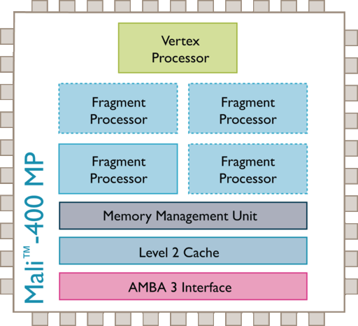
EDIT; I have found a very high up over view of Mali 400 from Exynos 4210..it shows AMBA 3 logic...is that an example of cache coherency using A9's??
Mali400-MP.gif


http://www.anandtech.com/show/4686/samsung-galaxy-s-2-international-review-the-best-redefined/16
It's called GeForce ULP. Tegra 3's size isn't that surprising when compared to Tegra 2's. TSMC's 40nm appears to allow some pretty damn dense stuff.
Even taking that into consideration, the GPU allocation is quite small...
Why on earth would you think the companion core wouldn't have NEON? That'd be disastrous.. look at the die shots, it's pretty much the same size as the other cores.
Well obviously you think other wise, but i did look at the die and thought i noticed that the companion core WAS smaller...could be wrong though.;)


Different processes, can't be compared. 7 year old PC architecture? I don't know what you think it's based on but I don't think it's based on anything. Also hard to call it the most powerful Android GPU out there when Adreno 225 is doing a pretty good job against it. Probably also without having to resort to lower resolution render targets, including depth buffer. And I don't see how it's a benchmark for performance, that one part of the market (Android) consists of SoCs that mostly haven't updated their GPUs in nearly as long.
The general consensus is that ULV Geforce is roughly based on Geforce 6 series...obviously chopped down somewhat similar to how Adreno 205 is roughly based on Xenos...If you catch my drift...And by the way, the Adreno 225 is a slightly weaker gpu IF you go by GL benchmark..even ramping up to 1080p...judging by a discusion with Ailuros..ULV Geforce has 2 pixel shaders and only 1 vertex shader??(Think thats right?) only 1-2TMU's 2 ROP's?...Adreno has something like 8 vect4 unified FP32 shaders...(not sure about other resources)..on paper the Adreno should smack the Geforce around..as it has not only twice the bandwidth. but less cpu's hogging it..also a much higher GFLOPS number, with unified shaders being more versatile...it just seems a much more effecient/modern design...both DX9.3 if im correct..


You're pulling that number completely out of thin air ;p.
Well sort of, i have seen a slide recently that mentioned 5x..don't ask me to link it because i can't find it:smile: but just taking the increased execution resources from having a bigger gpu (28nm) Unified shaders (rumoured to have a minimum of 24 'cores' whether thats ALU's like ULV Geforce..or proper vect4 FP32 shaders?)
- which i would imagine would be needed for DX 10+ class GPU's going forward...and probably OpenGL ES 3.0 Haiti also...they would be pretty stupid NOT to bring in a new architecture to align with W8 IMHO...not to mention dual channel memory + likely LPDDR3 to sit alongside.....its certainly not a stretch to be thinking 5x;)

EDIT; Links with '5x' improvement mentioned, Tegra 3 based on '8 year old pc architecture'..Kepler may be used....Also mentions 4+1 architecture would be used ....
http://vr-zone.com/articles/nvidia-tegra-4-to-get-gpgpu-i.e.-gpu-computational-capabilities-kepler-inside-/15361.html
 
Last edited by a moderator:
Would the supposed 5th LP A15 even need L2 cache? On Tegra 3, the LP core is supposedly only active when the screen is off, so I reckon the relatively rare L2 cache flushes wouldn't be a big deal.
 
My point still stands for non-A9 designs that utilize vSMP, however. Including, say, Wayne.

L2 is tightly coupled everywhere else and probably difficult to mix LP vs GP.. but on big.LITTLE L2 isn't shared (and afaik doesn't have to be the same size on the little cluster) and I'm sure you can make that cluster LP.

What's the fallout of having a cache maintenance op no-oping? Or even faulting. Aren't most OS's able to handle that?

Cache maintenance operations include flushes and invalidations. There are versions that work by set/way and therefore you need to know the cache size and associativity to use them. It's important that they actually work instead of NOPing (much less faulting, an implementation of ARMv7a can't add faults where the spec doesn't call for it) because otherwise you can end up with a stale cache causing incoherencies.

To compete with the ARM SoC's, IB would just need to be binned lower, say ~1.2GHz dual-core at sub 1V. That's perfectly feasible for reaching sub-10W. Whether or not Intel will do that, I don't know. But Windows-on-ARM is going to open up a whole market for them and, IMO, they'd be fools not to take it.

Should they really be trying to take that market with IB and not Atom? At what point does perf/W scaling on IB reach diminishing returns and make no sense vs the much cheaper Atom chips?

IIRC, there would still be a market for ~600-900 tablets provided they were fully functional Windows tablets with a slick tablet UI and ecosystem. Intel-based laptops nowadays can be sold for sub-$400 even.

We'll see - I personally don't think that market potential is that much bigger than the market for Windows 7 tablets is right now. Because I don't think that many people are looking for tablets that are both top of class as far as conventional tablets go and run legacy x86 apps. People view the two things as pretty separate..

And good luck finding a 17W (or less) IB laptop for sub $400. That market is dedicated to Brazos, Atom, maybe higher end AMD APUs, and maybe heavily crippled Celerons.

The price issue with ARM SoC's have more to do with economy of scale and lack of willingness on the OEM's part to accept not-like-Apple profit margins.

Bringing a more PC model to that market (razor thin margins, high volume) can take away the price issue.
What price issue with ARM SoCs? You're saying ARM SoCs are too expensive? Or tablets are too expensive? Because the latter is obviously already shifting with tablets like Kindle Fire. It isn't any longer a matter of not being able to accept razor thin margins and high volume; once you're already on that model going with a $100+ high end (non-Atom) Intel chip is going to be a hard sell vs a $20 ARM SoC.

Have no idea what you're getting at with the Grey stuff still, sorry ;p
 
EDIT; I have found a very high up over view of Mali 400 from Exynos 4210..it shows AMBA 3 logic...is that an example of cache coherency using A9's??

The AMBA 3 bus doesn't have anything for coherency. The Mali-400 in Exynos 4210 is therefore not cache coherent with the Cortex-A9 cores. So far GPUs rarely have been, even in APUs from AMD.

The general consensus is that ULV Geforce is roughly based on Geforce 6 series...obviously chopped down somewhat similar to how Adreno 205 is roughly based on Xenos...If you catch my drift...

General consensus is often formed from people who don't really know what they're talking about >_> People are probably just seeing that it's non-unified and DX9 level and drawing conclusions from there. There's a lot more to it than that.

And by the way, the Adreno 225 is a slightly weaker gpu IF you go by GL benchmark..even ramping up to 1080p...judging by a discusion with Ailuros..ULV Geforce has 2 pixel shaders and only 1 vertex shader??(Think thats right?) only 1-2TMU's 2 ROP's?...Adreno has something like 8 vect4 unified FP32 shaders...(not sure about other resources)..on paper the Adreno should smack the Geforce around..as it has not only twice the bandwidth. but less cpu's hogging it..also a much higher GFLOPS number, with unified shaders being more versatile...it just seems a much more effecient/modern design...both DX9.3 if im correct..

Adreno 220/225 should be 4 vec4 FP32 unified ALUs. But of course there are a lot of fine details that dominate comparisons. nVidia probably still has better drivers too.

EDIT; Links with '5x' improvement mentioned, Tegra 3 based on '8 year old pc architecture'..Kepler may be used....Also mentions 4+1 architecture would be used ....
http://vr-zone.com/articles/nvidia-tegra-4-to-get-gpgpu-i.e.-gpu-computational-capabilities-kepler-inside-/15361.html

You really shouldn't be taking Theo Valich's speculation as authoritative or even informed. Saying that removing the (rather sparse) FP64 cores will bring down power massively is pretty damn silly, given that they weren't being used in most power measurements to begin with.. Not good that he doesn't even understand the FP64 layout of Fermi vs Kepler either.. He also thinks OMAP6 will use Mali and 4x Cortex-A15 Exynos will use PowerVR o_o
 
Would the supposed 5th LP A15 even need L2 cache? On Tegra 3, the LP core is supposedly only active when the screen is off, so I reckon the relatively rare L2 cache flushes wouldn't be a big deal.

It's active any time you need only one core that can be <= 500MHz. It could literally be triggered on what you set the clock speed to. This could often be used when the screen is on. One of the reasons this is preferable to having a core hurry up and sleep is that it's less sensitive to things like interrupts having to wake it up/ramp it all the time.

L2 cache is actually a big perf/W benefit, even a small amount will lower power consumption a lot for the same workload. Main memory performance is no small hit on these platforms. It's hard to imagine actually wanting an A15 with no L2 cache in any real world situation. Which is probably why ARM doesn't even appear to offer such a thing: http://infocenter.arm.com/help/index.jsp?topic=/com.arm.doc.ddi0438d/BABJCGGE.html
 
Back
Top