NVIDIA Tegra Architecture

Why didn't they roll with A72's? Or is that just a marketing thing.

My guess is that there was faster time to integration because they could leverage past work done on X1. They could have tacked on the A57s relatively late, when they realized they weren't winning enough benchmarks anymore with the Denver cores alone.
 
Did anyone get confirmation about the 2.5 TFlops figure from Nvidia, or is everyone just basing it on the same spec page? Because as stupid as it sounds, even to me if I think about it twice, I came up with a little "theory": it's a typo and should say 3.5 TFlops. Coincidentally that would make it 52% higher than TX1 and clocks would be 1.7 Ghz, which is kinda high, but Drive PX1 was also clocked realtively high even by Maxwell standards and it's not really high by Pascal standards.
 
No I am not. I thought the allusion I made was pretty clear, but apparently I need to spell it out. The clocks used in PX2 may not be any higher than the reference X2. But I am done here, believe what you will...
I think you misundertand my context and does not help you cut the sentence and its full meaning as well.
Sorry you feel this is turning into an argument but it is not 25% clock bump when comparing like for like (this is the only real world comparison we can currently do) but actually 8.5%.
And that is all either of us can say for now until we get information about the reference X2, to say otherwise is speculation.

Cheers
 
Did anyone get confirmation about the 2.5 TFlops figure from Nvidia, or is everyone just basing it on the same spec page? Because as stupid as it sounds, even to me if I think about it twice, I came up with a little "theory": it's a typo and should say 3.5 TFlops. Coincidentally that would make it 52% higher than TX1 and clocks would be 1.7 Ghz, which is kinda high, but Drive PX1 was also clocked realtively high even by Maxwell standards and it's not really high by Pascal standards.

Talking about typos,
I finally worked out why Nvidia responded to Computerbase.de about the 1.5 TFLOPS FP16 being wrong (I just realised Computerbase.de do mention it in their article), Nvidia put that figure in their blog page and still not corrected it yet lol.
Built around NVIDIA’s highest performing and most power-efficient Pascal GPU architecture and the next generation of NVIDIA’s revolutionary Denver CPU architecture, Parker delivers up to 1.5 teraflops(1) of performance for deep learning-based self-driving AI cockpit systems..
..
  1. References the native FP16 (16-bit floating-point) processing capability of Parker.
.
https://blogs.nvidia.com/blog/2016/08/22/parker-for-self-driving-cars/
Regarding the figures, if it had 3.5 TFLOPS then the official 24DL TOPS really breaks down and becomes 27DL TOPS.
That figure only works with 2.5 TFLOPS FP16 with the discrete GPUs that are 5 TFLOPS FP32.

Cheers
 
I think you misundertand my context and does not help you cut the sentence and its full meaning as well.
I haven't misunderstood anything.

Sorry you feel this is turning into an argument but it is not 25% clock bump when comparing like for like
It is not an argument. It is you choosing to maintain a purposefully obtuse perspective. But like I said before, that is your business not mine... It is simply not my or anyone else's problem but your own. Good luck with that.
 
I haven't misunderstood anything.

It is not an argument. It is you choosing to maintain a purposefully obtuse perspective. But like I said before, that is your business not mine... It is simply not my or anyone else's problem but your own. Good luck with that.
OK one last time without insults please and we can move on.
Please tell me the clock speed for both the Drive PX and the Drive PX2; you agree it is 1.15 and 1.25 when going by Nvidia's figures of 2.3 TFLOPS and 2.5 TFLOPS?
Now tell me why it is ok to compare the Drive PX2 to the totally different non-platform reference TX1 (that has standard clocks at 1GHz) when we do not know what the reference 'X2' will be.
Thanks
 
Talking about typos,
I finally worked out why Nvidia responded to Computerbase.de about the 1.5 TFLOPS FP16 being wrong (I just realised Computerbase.de do mention it in their article), Nvidia put that figure in their blog page and still not corrected it yet lol.

And if it's wrong, then what is the correct number, Nvidia? Dang it.

Regarding the figures, if it had 3.5 TFLOPS then the official 24DL TOPS really breaks down and becomes 27DL TOPS.
That figure only works with 2.5 TFLOPS FP16 with the discrete GPUs that are 5 TFLOPS FP32.

And what are those DL TOPS really? First I thought it was FP16, then INT8, but now I have no idea whatsoever. Also I don't know how to get 24 from either "2.5 + 5" or "2.5 + 10" or whatever.
 
And if it's wrong, then what is the correct number, Nvidia? Dang it.


And what are those DL TOPS really? First I thought it was FP16, then INT8, but now I have no idea whatsoever. Also I don't know how to get 24 from either "2.5 + 5" or "2.5 + 10" or whatever.
Some form of Int8, like we see with the Pascal Titan X although that is called Int8 TOPS.
Both relate to inferencing in Deep Learning I would say.

So the dual discrete GPUs provides 5 TFLOPS FP32 = 20 DL TOPS.
The dual Tegra 'X2' provides 2.5 TFLOPS FP16 = 5 DL TOPS.
So yeah that is 25 instead of 24 DL TOPS but as close as you can get to the summary figures.
Cheers
 
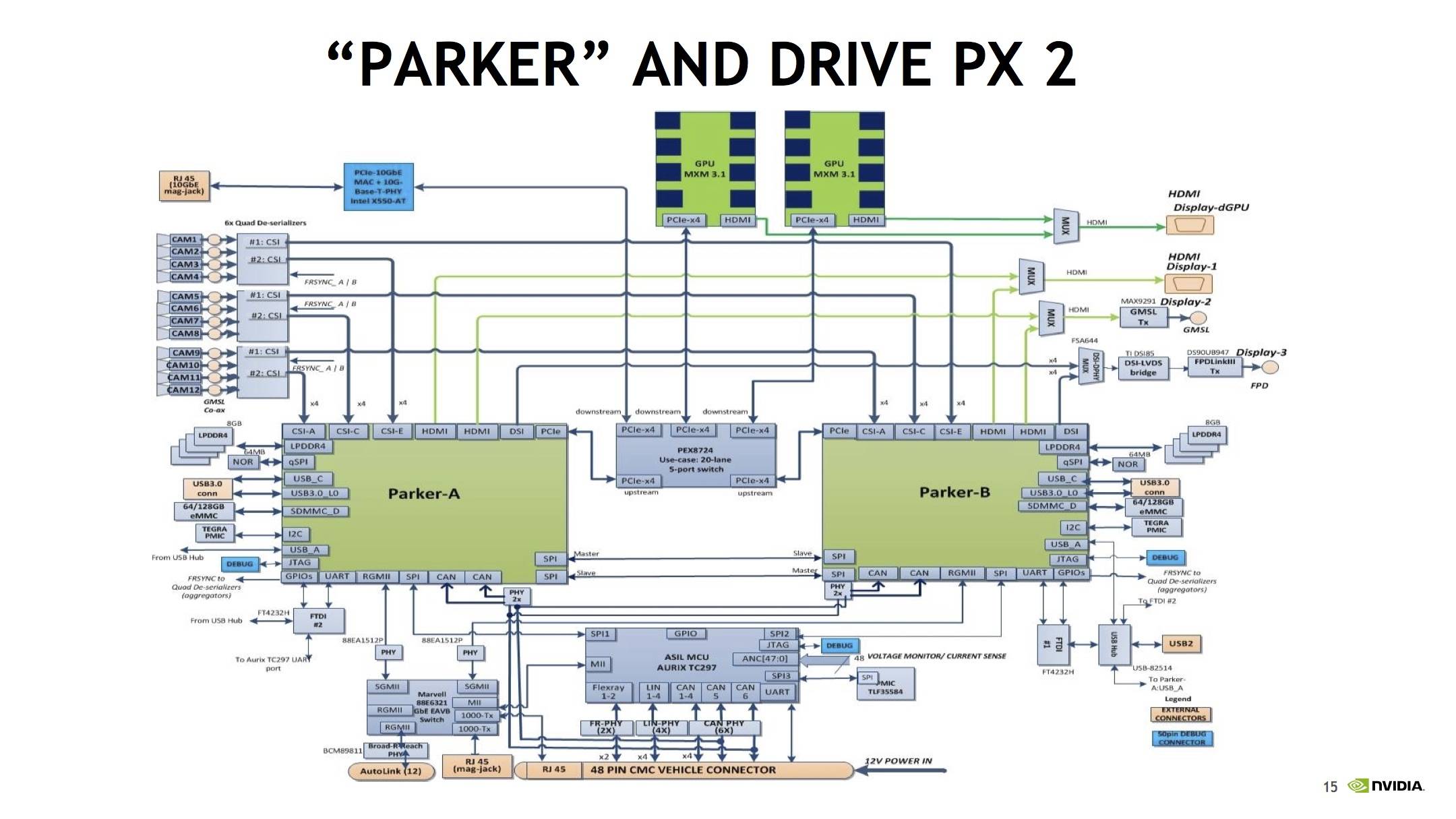
Drive PX2 block diagram
nvidia_parker_4.jpg
 
Some form of Int8, like we see with the Pascal Titan X although that is called Int8 TOPS.
Both relate to inferencing in Deep Learning I would say.

So the dual discrete GPUs provides 5 TFLOPS FP32 = 20 DL TOPS.
The dual Tegra 'X2' provides 2.5 TFLOPS FP16 = 5 DL TOPS.
So yeah that is 25 instead of 24 DL TOPS but as close as you can get to the summary figures.
Cheers

So it's int8 after all.

IDK about the 24 = 25. Doesn't really satisfy me. Seems kinda far fetched as any other guess we are making. Also wasn't that figure the old one (January?) that came along with the 8 TFlops FP32 figure? Even back then, 8 TFlops and 24 DL TOPs didn't really work very well. I think that we're missing something (a lot really). Also if you remember, when the PX2 was annpounced the board that was shown had GP106s. So I don't think the 8 TFlops and 24 DL TOPs figure is actually relevant anymore TBH.
Note the GPUs have never been specified so cannot really consider them as GP106 with this final product, that also needs clarifying at some point.
Worth noting the GP106 at 61W can still hit its base 1500MHz clocks and that would be 3.8 TFLOPS for a single GPU, that would be pretty bad dual setup scaling for 5 TFLOPS but then again more information is needed on how the dual Tegra/dual GPU works as it looks like a discrete GPU is dedicated to each Tegra processor.

But yeah you probably seen my own views about the specifications reported so far from slides, the Nvidia site, and also their response to Computerbase.de.
And yeah some of the figures given back some time ago for the Drive PX 2 are possibly no longer applicable, such as the 250W power.

The 24DL TOPS could had originally been based upon using the Drive PX X1 clocks and TFLOPS, that would then give you 24.6 DL TOPS and since then increased the clocks a bit to give 2.5 TFLOPS now.
But like you would like more information.
Cheers
 
Well, the biggest single chunk will come from the +100% bandwidth advantage. The 2 Denver2 CPUs will also help a fair amount I imagine. The rest is probably a bunch of small stuff (arch) and clocks. But I really don't see why they couldn't clock the GPU at 1.4 GHz (like they do in laptops...) for automotive applications or anywhere it is going to be plugged in...

A theoretical frequency increase for the GPU of 22% plus the sizeable increase in bandwidth sounds at least for me enough to do the trick to reach a 50% efficiency increase.

As for higher clocks I'd personally prefer with something as crucial as automotive which obviously can involve ADAS too for any IHV to stay on the "120%" safe side, instead of taking even the tiniest risk.

I'm curious to see if Denver2 is a significant architectural overhaul or simply a quick revamp to yield the certicifations Denver Prime couldn't yield.

Perhaps they haven't, or at least wanted to leave that door open. Generally, maintaining open doors is a poor strategy, but if anybody can afford to do it....

I think we all can agree that it's unlikely that we'll see anytime soon any new Tegra SoC in any kind of smartphone. At least we can close that chapter for good for now. For every other high end solution above that I don't see why they would say "no" to any opportunity that will come up and prove for that is the Nintendo NX deal.
 
I'm curious to see if Denver2 is a significant architectural overhaul or simply a quick revamp to yield the certicifations Denver Prime couldn't yield.
I doubt it is anything terribly significant in terms of design. There might be some nice performance bumps for specific situations though. I do think Nvidia would probably be better off to just transition solely to ARM, whether that is an evolution of Denver or A72. If they were genuinely interested in pursuing the x86 market, they should have bought AMD when they had the chance. As it is now, I can't see the value of maintaining/evolving Denver in its current form, unless there is some really significant perf/watt advantages to be had (which I doubt). The A72 is already quite good.

I think we all can agree that it's unlikely that we'll see anytime soon any new Tegra SoC in any kind of smartphone. At least we can close that chapter for good for now. For every other high end solution above that I don't see why they would say "no" to any opportunity that will come up and prove for that is the Nintendo NX deal.
Agreed. I think they may eventually try another crack at cell phones once HBM2 or whatever the mobile equivalent is becomes common place because that is when their value add can really shine. But I wouldn't be surprised if they take a more Apple approach of just selling a phone directly.
 
I doubt it is anything terribly significant in terms of design. There might be some nice performance bumps for specific situations though. I do think Nvidia would probably be better off to just transition solely to ARM, whether that is an evolution of Denver or A72.

I do not believe that Nvidia would be better off with plain ARM cores that everyone will copy.
 
Going ARM and being custom designs are not mutually exclusive, see Qualcomm, Apple, etc....

And it is axiomatic that they would be better served with using a reference design, if that reference design is just better in every way.
 
Back
Top