Install the app
How to install the app on iOS
Follow along with the video below to see how to install our site as a web app on your home screen.
Note: This feature may not be available in some browsers.
You are using an out of date browser. It may not display this or other websites correctly.
You should upgrade or use an alternative browser.
You should upgrade or use an alternative browser.
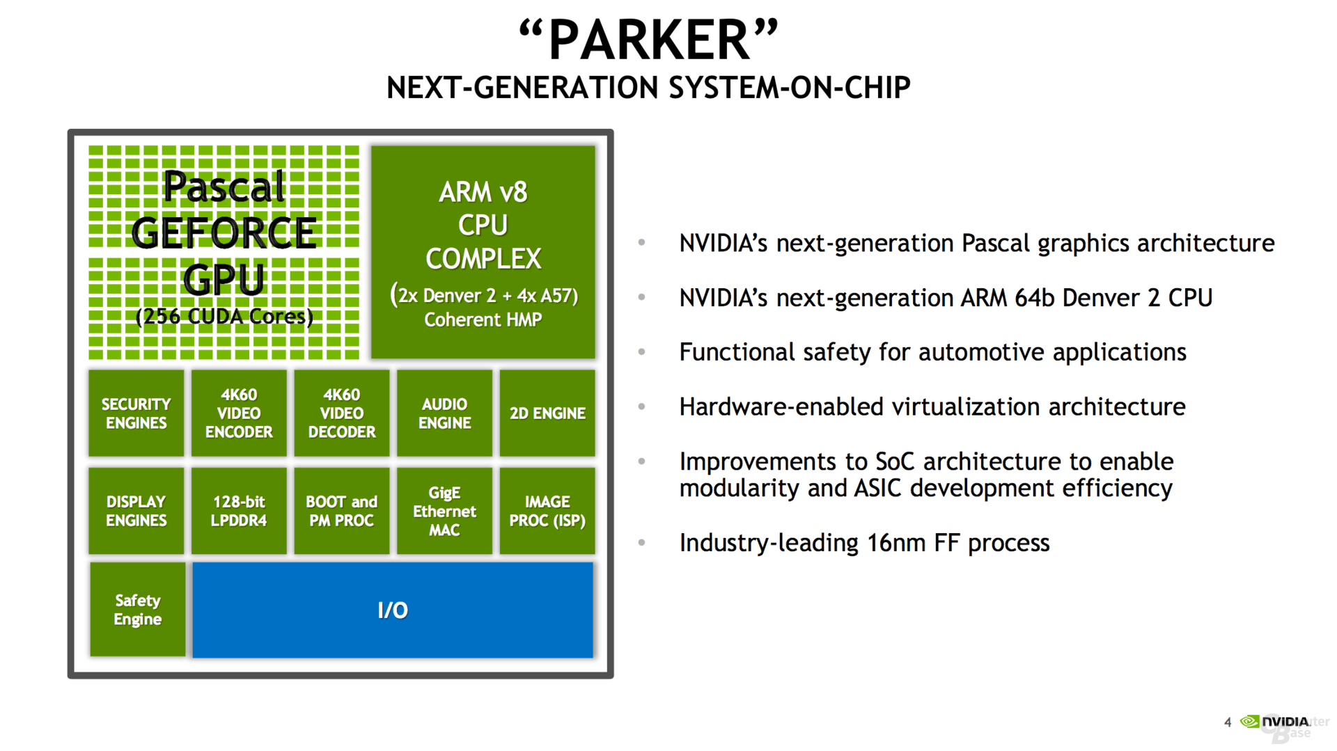
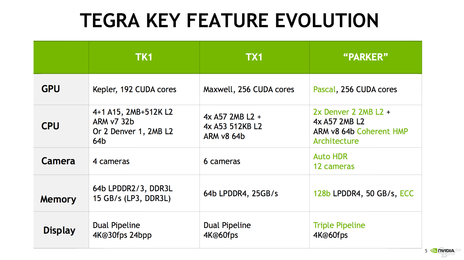
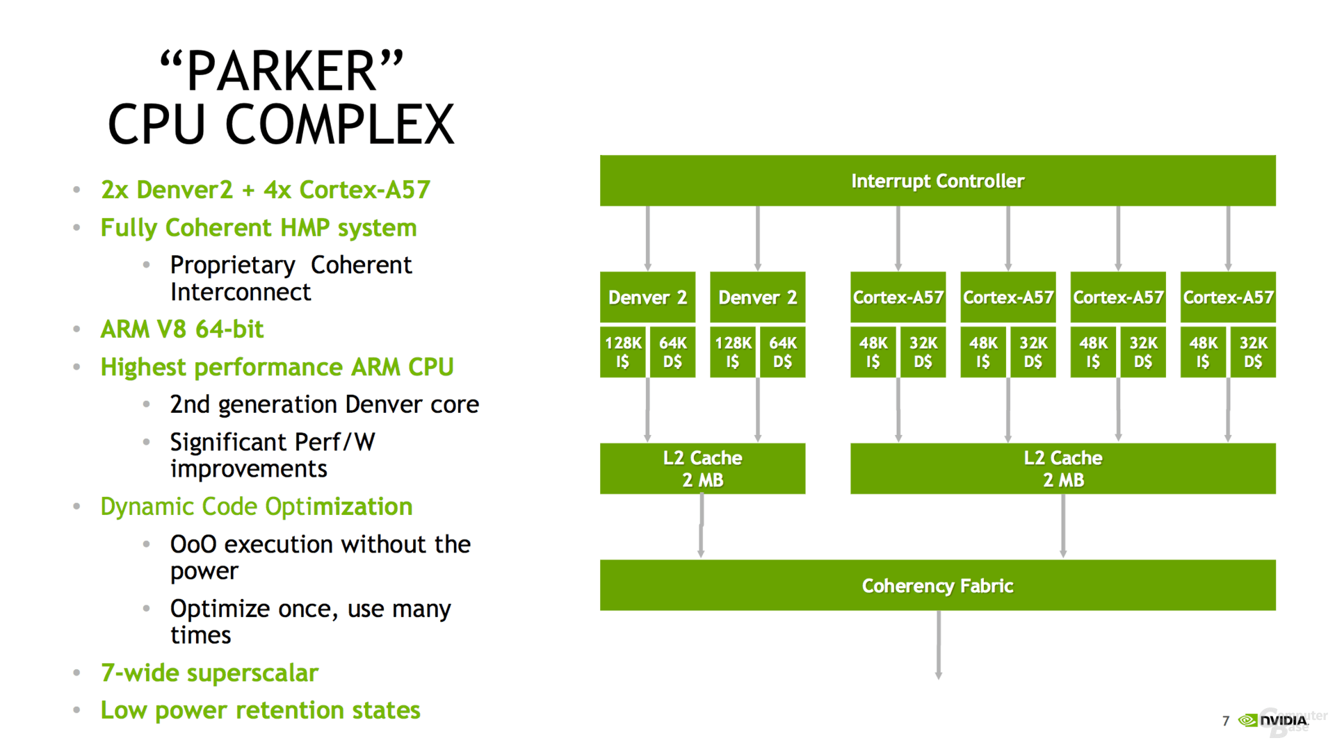
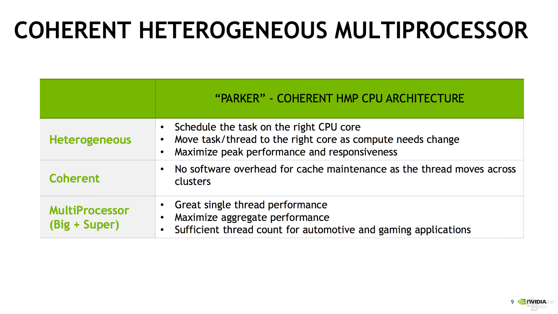
NVIDIA Tegra Architecture
- Thread starter french toast
- Start date
-
- Tags
- nvidia
Rikimaru
Veteran
It is not a good mobile chip. That's a reason.
https://twitter.com/fioraaeterna/status/757955789503868928
https://twitter.com/fioraaeterna/status/757955789503868928
If by "not good mobile chip" you define a more efficient SOC than Apple A8X that was praised in its moment... then yeah.It is not a good mobile chip. That's a reason.
https://twitter.com/fioraaeterna/status/757955789503868928
And they have Finfet to develop a new chip now
It is not a good mobile chip. That's a reason.
https://twitter.com/fioraaeterna/status/757955789503868928
The X1 seems unlikely to be the SoC of choice as it and 20nm are basically EoL.
Though even if they did pick the X1, it would only take a modest underclock and undervolt for it to be suitable in both power consumption and performance requirements.
monstercameron
Newcomer
The X1 seems unlikely to be the SoC of choice as it and 20nm are basically EoL.
Though even if they did pick the X1, it would only take a modest underclock and undervolt for it to be suitable in both power consumption and performance requirements.
Is tsmc 20nm eol?
If you care about efficiency and battery life....
Short-term, I believe the costs/transistor are about equal maybe slightly cheaper for 20nm. Of course, 16nm FF is going to save die size while also offering a power, heat, and performance advantage. So long-term 16nm FF makes much more sense...
Short-term, I believe the costs/transistor are about equal maybe slightly cheaper for 20nm. Of course, 16nm FF is going to save die size while also offering a power, heat, and performance advantage. So long-term 16nm FF makes much more sense...
Last edited:
"More efficient" how? Shield console has a fan in it. No Ax CPU device Apple ever made has had a fan. iPhones in general also experience far less clock throttling than basically any other comparable smartphone, and that's without resorting to strapping a heatpipe to the SoC like many phones have to do these days.If by "not good mobile chip" you define a more efficient SOC than Apple A8X that was praised in its moment... then yeah.
Is tsmc 20nm eol?
No. But popularity and production are lower than 16nm.
If you care about efficiency and battery life....
Short-term, I believe the costs/transistor are about equal maybe slightly cheaper for 20nm. Of course, 16nm FF is going to save die size while also offering a power, heat, and performance advantage. So long-term 16nm FF makes much more sense...
Cost/transistor is a fair bit cheaper for 20nm. And the die size reduction of 16FF is insignificant (Not that it matters when cost/transistor is higher). For a mobile device, the power and/or performance are far more important and worth the higher cost.
"More efficient" how? Shield console has a fan in it. No Ax CPU device Apple ever made has had a fan. iPhones in general also experience far less clock throttling than basically any other comparable smartphone, and that's without resorting to strapping a heatpipe to the SoC like many phones have to do these days.
The Tegra X1 does have significantly higher performance than A8X though so its not an apples to apples comparison. At iso performance, the TX1 GPU is more efficient than A8X - http://www.anandtech.com/show/8811/nvidia-tegra-x1-preview/3 (Take that with an appropriate dose of salt though..those numbers are from NV and I dont believe they have been independently verified)
I question the statement about 20nm being a fair bit cheaper than the FinFet variant. All the calculations I've seen seem to base that on lower yields from 16nmFF vs. 20nm planar, and I don't think that's a valid assumption anymore, never mind developments such as the cost optimised 16nm FFC. But I've struggled to find numbers that are both unbiased and up to date, so if you have a good source, I'd love to take a look.No. But popularity and production are lower than 16nm.
Cost/transistor is a fair bit cheaper for 20nm. And the die size reduction of 16FF is insignificant (Not that it matters when cost/transistor is higher). For a mobile device, the power and/or performance are far more important and worth the higher cost.
As far as I can see 20nm was a stepping stone process, and at this point in time is pretty much superceded by the FinFet variant that offers vastly better performance.
The only reason I can see for Nintendo using a 20nm Tegra is if nVidia has a lot of otherwise unsellable stock, in amounts that would cover a fair bit of projected lower bound of NX total sales volume. In any other scenario, it would benefit nVidia and Nintendo both more to get higher volume on the 16nm product.
I question the statement about 20nm being a fair bit cheaper than the FinFet variant. All the calculations I've seen seem to base that on lower yields from 16nmFF vs. 20nm planar, and I don't think that's a valid assumption anymore, never mind developments such as the cost optimised 16nm FFC. But I've struggled to find numbers that are both unbiased and up to date, so if you have a good source, I'd love to take a look.
As far as I can see 20nm was a stepping stone process, and at this point in time is pretty much superceded by the FinFet variant that offers vastly better performance.
The only reason I can see for Nintendo using a 20nm Tegra is if nVidia has a lot of otherwise unsellable stock, in amounts that would cover a fair bit of projected lower bound of NX total sales volume. In any other scenario, it would benefit nVidia and Nintendo both more to get higher volume on the 16nm product.
Sorry..I cant give you any public source for that. However, simply put..ask yourself how 16FF can have a lower per transistor cost despite being a more complex process with no significant die size reduction (That is the key here. 16FF is more like 20FF. An actual full node transition like Intel 22nm to 14nm does have lower transistor cost and we will see the same with 16/14nm to 10nm). There are commercial aspects to it as well. I'll have to look into 16FFC with a bit more detail but I have my doubts.
If you blink all eyes for power consumption and/or perf/mW then yes 20SoC could be a "better" choice vs. 16FF+
http://www.anandtech.com/show/9762/hisilicon-announces-kirin-950-huawei
Here the "it is struggling" slide from Huawei is an eye opener and I doubt there's even one industry insider that will tell you otherwise:
http://images.anandtech.com/doci/9762/P1030606.jpg?_ga=1.132281870.1879829433.1453271737
http://www.anandtech.com/show/9762/hisilicon-announces-kirin-950-huawei
Here the "it is struggling" slide from Huawei is an eye opener and I doubt there's even one industry insider that will tell you otherwise:
http://images.anandtech.com/doci/9762/P1030606.jpg?_ga=1.132281870.1879829433.1453271737
The thing is that 16FF isn't a significantly more complex process than 20nm planar, which already took the multiple patterning hit, plus the overall issues surrounding a shrink. If you want to be a bit uncharitable, you could say that 28nm planar to 16nmFF was a single generation, taken in two steps - one in density, and the other in fundamental transistor design (FF). Once the full transition has been made, the interim step, 20SoC, has little to recommend it.Sorry..I cant give you any public source for that. However, simply put..ask yourself how 16FF can have a lower per transistor cost despite being a more complex process with no significant die size reduction (That is the key here. 16FF is more like 20FF. An actual full node transition like Intel 22nm to 14nm does have lower transistor cost and we will see the same with 16/14nm to 10nm). There are commercial aspects to it as well. I'll have to look into 16FFC with a bit more detail but I have my doubts.
http://www.nvidia.com/object/drive-px.html
- Scalable from 1 to 4 processors (2 next generation Tegra SoC and 2 Pascal GPUs)
- Dual NVIDIA Tegra® processors delivering a combined 2.5 Teraflops
- Dual NVIDIA Pascal discrete GPUs delivering over 5 TFLOPS and over 24 DL TOPS
- Interfaces for up to 12 cameras, radar, lidar, and ultrasonic sensors
- Periodic software/OS updates
http://www.nvidia.com/object/drive-px.html
- Scalable from 1 to 4 processors (2 next generation Tegra SoC and 2 Pascal GPUs)
- Dual NVIDIA Tegra® processors delivering a combined 2.5 Teraflops
- Dual NVIDIA Pascal discrete GPUs delivering over 5 TFLOPS and over 24 DL TOPS
- Interfaces for up to 12 cameras, radar, lidar, and ultrasonic sensors
- See more at: http://www.nvidia.com/object/drive-px.html#sthash.auXSPWNS.dpuf
- Periodic software/OS updates
Good find. Points to a 3 SM, 384 CC GPU for the Tegra SoC, and clocked fairly high (~1.4 Ghz would be my guess)
Benetanegia
Regular
Good find. Points to a 3 SM, 384 CC GPU for the Tegra SoC, and clocked fairly high (~1.4 Ghz would be my guess)
Correct me if I'm wrong but that'd fall incredibly short for the 1.25 TFlop per Tegra SoC claim.
384 x 2 x 1.4 = 1075
It'd need 1.6 Ghz to reach 1.25 TFlops, which seems unlikely to me. Then again for 512 CC it would be like 1.2 Ghz or so? Maybe too low for a Pascal, but more realistic IMO.
EDIT: At 1.25 TFlops (assuming FP32) it's a beast, regardless.
You aren't wrong. I was counting the CPUs as well. I assumed ~1.1 TFlops from each GPU and 150 Gflops from the CPUs (4xA57 + 2xDenver) so ~1.25 Tflops per SoC
Benetanegia
Regular
You aren't wrong. I was counting the CPUs as well. I assumed ~1.1 TFlops from each GPU and 150 Gflops from the CPUs (4xA57 + 2xDenver) so ~1.25 Tflops per SoC
Hmm fair enough. Nvidia didn't count CPU Flops in previous SoCs tho, which is not to say they wouldn't start now.
Good find. Points to a 3 SM, 384 CC GPU for the Tegra SoC, and clocked fairly high (~1.4 Ghz would be my guess)
Why not ~1.2GHz for everything? 4*128SPs (8*64 sounds unlikely) for each Parker SoC GPU and 8*128 for each GP106. A loooooong time ago when I asked the answer was along "over 1GHz for everything" which if it wasn't just random BS and their target frequencies were at 1100+, reaching 1200 after tape out is quite feasable.
Similar threads
- Replies
- 10
- Views
- 827
- Locked
- Replies
- 10
- Views
- 1K
- Replies
- 0
- Views
- 772
- Replies
- 11
- Views
- 3K
- Replies
- 90
- Views
- 18K