Install the app
How to install the app on iOS
Follow along with the video below to see how to install our site as a web app on your home screen.
Note: This feature may not be available in some browsers.
You are using an out of date browser. It may not display this or other websites correctly.
You should upgrade or use an alternative browser.
You should upgrade or use an alternative browser.
NVIDIA Tegra Architecture
- Thread starter french toast
- Start date
-
- Tags
- nvidia
D
Deleted member 13524
Guest
nVidia could simply point to a "modest" 1.6x performance upgrade and aim to have its SoC available to phablets and larger smartphones.
nVidia could simply point to a "modest" 1.6x performance upgrade and aim to have its SoC available to phablets and larger smartphones.
Could be. Realistically the Shield tablet has already broken the 30fps "barrier" in Manhattan and it doesn't look like there's all that much in sight to surpass that sort of performance any time soon. The question would be who needs over twice as much even just in theory next year?
Could be. Realistically the Shield tablet has already broken the 30fps "barrier" in Manhattan and it doesn't look like there's all that much in sight to surpass that sort of performance any time soon. The question would be who needs over twice as much even just in theory next year?
I'll admit that I don't know too much about the mobile gaming scene but is anyone actually asking for faster graphics on their phone or tablet? If they are asking for it my next question is what games are they playing.
nVidia's console mode is an interesting approach to driving demand for faster SoC's but for mainstream usage I don't quite get it. At some point good enough is going to be good enough.
For sure someone could say that they might want to drive console or PC ports into the ULP mobile space, but in order for that to work out ISVs still would need good enough marketshare to start porting a multitude of games for those tablets. Less of a handful of games won't obviously cut the cake.
GK20A@K1 has set very strong foundations (DX11, double precision, high performance) for a ULP SoC GPU. With Maxwell you can have the same package at way less power consumption. If you hold in one hand a solution that does way over 60fps in Manhattan but lasts roughly two hours and in the other hand a solution that slighly increases over 30fps but lasts way over 5 hours, guess which one the majority would prefer.
Blazkowicz
Legend
Would Erista simply have one SMM?
Keep it simple for lowest complexity and power use.
Now by stealing ams's numbers that gives :
Tegra K1: 192
Tegra M1: 128
Performance worsening with Tegra M1 Erista: 0.6667x
Performance per CUDA core
Performance improvement with Tegra M1 Erista: 1.400x
Peak GPU clock operating frequency
Performance improvement with Tegra M1 Erista: 1.218x
Overall : +13.7% performance at peak.
With increased perf/watt, more real world performance than that.
The 1.4x performance per CUDA core is btw another way of saying that an SMM has about the same performance as an SMX")
Keep it simple for lowest complexity and power use.
Now by stealing ams's numbers that gives :
Tegra K1: 192
Tegra M1: 128
Performance worsening with Tegra M1 Erista: 0.6667x
Performance per CUDA core
Performance improvement with Tegra M1 Erista: 1.400x
Peak GPU clock operating frequency
Performance improvement with Tegra M1 Erista: 1.218x
Overall : +13.7% performance at peak.
With increased perf/watt, more real world performance than that.
The 1.4x performance per CUDA core is btw another way of saying that an SMM has about the same performance as an SMX
@ Blazkovicz: Erista will need two SMM's (ie. 256 CUDA cores in total) to actually significantly improve in performance vs. Tegra K1. Theoretically one SMM is possible, but I just don't see them going that route @ the 20nm fab. process node where transistor density is vastly improved vs. 28nm HPM.
@ Blazkovicz: Erista will need two SMM's (ie. 256 CUDA cores in total) to actually significantly improve in performance vs. Tegra K1. Theoretically one SMM is possible, but I just don't see them going that route @ the 20nm fab. process node where transistor density is vastly improved vs. 28nm HPM.
Depends what they have actually planned; if they don't have another 121mm2 SoC in mind but something that's quite a bit below 100mm2 what then?
Besides since someone from ARM also mentions here that for 20SoC leakage is too high for the performance gain, which is roughly inline what I had heard for the process quite some time ago:
http://www.google.de/url?sa=t&rct=j&q=&esrc=s&source=web&cd=1&cad=rja&uact=8&ved=0CCUQFjAA&url=http%3A%2F%2Fwww.ispd.cc%2Fslides%2F2014%2Fkeynote_Aitken.pptx&ei=FLMzVPmHJ8jFPZKZgJgK&usg=AFQjCNEyAtm_y-Wrf7P0211pz2kZqYb5mQ&bvm=bv.76943099,d.ZWU
I'm not saying they have gone in that direction, but it's not that absurd as a theory.
iMacmatician
Regular
Are we ruling out the possibility of one Erista chip with 1 SMM and another with 2 SMMs?
Are we ruling out the possibility of one Erista chip with 1 SMM and another with 2 SMMs?
As Nvidia have publicly stated that the low to mid-end smartphone market is too cutthroat for them to contemplate a replacement for the Tegra 4i, I cannot see where a 1 SMM Erista would fit into their product lineup. If Nvidia wants to cement the gaming / performance tablet market they need to keep pushing the GPU perf envelope, at the very least for the PR spin it creates.
So did Xiaomi sell 50K MiPads in a few hours because of anything else but "Keplar" inside?
50k isn't that much. Besides..their main selling point is price rather than anything else. They sold 60k Redmi 1s in 13 seconds in India.
If you look at the latest "highend" china-phones they start to use the new MT6595 a lot. Maybe the Antutu benchmark results of >45000 are enough for them.
They may call themselves "high end", but the reality is that they are nothing more than glorified mid-range phones. Personally, if it dosen't have at least a Snapdragon 800 or a quad Cortex A15, it isn't high end.
yes, it seems nvidia didn't want to use Denver for servers. So they have the SoC but now instead of pushing it they stopped. This seems to imply that they have given up on servers.
Any source to this?
Peak GPU clock operating frequency
Tegra K1: 852MHz
Tegra M1: 1038MHz
Performance improvement with Tegra M1 Erista: 1.218x
Overall graphics performance improvement with Tegra M1 Erista vs Tegra K1 Logan at the same power envelope: 2.27x !!!
What are you basing the M1 clock from? From what I've read and heard, 20SoC will basically offer the same performance as 28 HPM, but with a minor decrease in power.
Would Erista simply have one SMM?
Keep it simple for lowest complexity and power use.
Wouldn't two SMMs at lower clocks be more power efficient than one higher clocked SMM? They wouldn't really be die constrained as 20SoC would allow much higher density.
That aside, the performance would not be good enough IMHO..they would be targeting at least a 50% improvement from one generation to the next.
Are we ruling out the possibility of one Erista chip with 1 SMM and another with 2 SMMs?
Did we ever consider it? There is no precedent to this by Nvidia..and besides there is little point in creating two SoCs with such a small difference (Not unless you have considerable volume..which Nvidia admittedly dosen't..and even then its questionable).
That's kind of his point..Nvidia has stated that they will not compete in this market and will target high end only..so a 1 SMM part is not good enough IMHO.Erm, a putative 1 SMM chip would still have extremely good GPU performance for the low-end to mid-range market, I'd have thought?
Last edited by a moderator:
1 or 2 SMM doesn't really make all that much of a difference considering the whole SoC size. So, unless it's a whole different SoC, it's probably not worth the trouble unless the volume is extremely high. Just disable 1 SMM if you want to sell some lower end chip...
Unless Maxwell ULP has "only" 1 quad TMU per SMM, if they go for 2 SMMs the typical 16 TMUs aren't exactly small either.
It's a pure gut feeling but I wouldn't estimate GK20A@K1 for less than 30mm2@28HPm and not under 400Mio transistors. Assuming that's not too far from reality a 2 SMM Maxwell ULP GPU could very well end up at least again at 30mm2@20SoC.
If NV keeps the same strategy as with K1 yes they probably used 2 clusters; if however they're aiming for a rather conservative overall performance increase but a quite high perf/W difference 1 cluster could also be a viable scenario.
I agree this could be an option, I just didn't agree that two versions made sense.If NV keeps the same strategy as with K1 yes they probably used 2 clusters; if however they're aiming for a rather conservative overall performance increase but a quite high perf/W difference 1 cluster could also be a viable scenario.
FWIW I don't share the views of some here it will be a >2x perf/w improvement based on some extrapolated desktop numbers, not least because I suspect not all power savings came from architecture changes but rather some lower level tweaks. Which most likely gk20a already all has anyway (even gk208 was quite a bit more power efficient already).
But it's going to be difficult to get much of a performance increase at all with just 1 SMM (at least for the larger form factors).
As Blackowitcz I would favor a single SMM and 2 CPU cores.
If they have silicon in spare it could be well spent on extra.cache both for the CPU and the GPU.
The comparison between the shield and the tegra note7 shows very well ow much throtling affects performances.
The tegra K1 offers plenty of performances, unchecked it could burn in the 30 Watts (Nvidia own numbers), even unchanged on a better process it would realize a lot more of its potential and with TDP fitting to a wider range of devices and by that I mean reaching Nvidia target market phones.
Last edited by a moderator:
FWIW I don't share the views of some here it will be a >2x perf/w improvement based on some extrapolated desktop numbers
I didn't extrapolate using desktop numbers. I used the single precision GFLOPS per watt data from NVIDIA's Tegra roadmap to determine the GPU perf. per watt ratio between Erista and Logan:
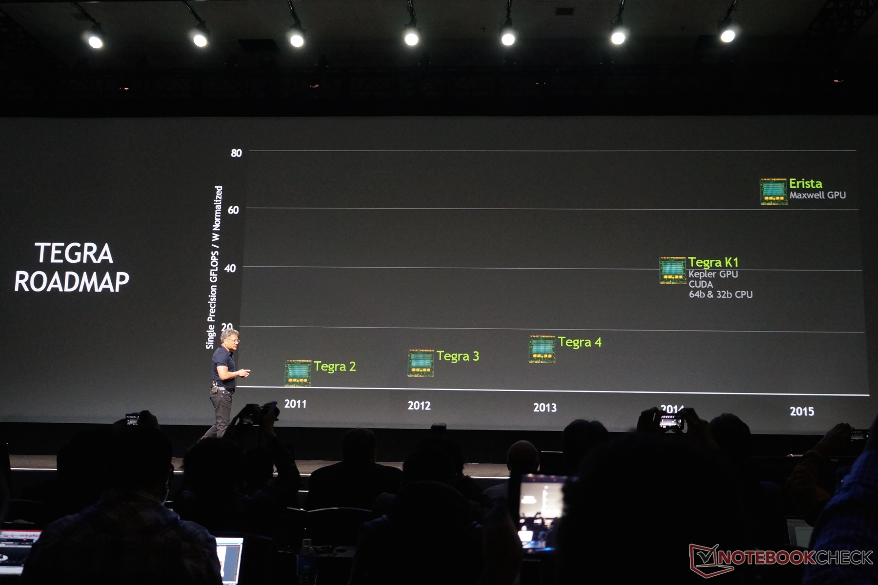
The improvement in GFLOPS per watt is ~ 1.625x for Tegra M1 Erista compared to Tegra K1 Logan. So at the same power consumption as Tegra K1 Logan (which has a peak throughput of ~ 327 GFLOPS at a peak GPU clock operating frequency of ~ 852MHz with 192 Kepler CUDA cores), Tegra M1 Erista will have a peak throughput of ~ 531 GFLOPS at a peak GPU clock operating frequency of ~ 1038MHz with 256 Maxwell CUDA cores, assuming that two SMM's are utilized).
Since a Maxwell CUDA core has ~ 1.4x higher graphics performance than a Kepler CUDA core, and hence 1.4x higher graphics performance per theoretical FLOP throughput, my estimate for overall graphics performance improvement of Tegra M1 Erista vs. Tegra K1 Logan at the same power consumption is ~ 2.27x.
On a side note, Tegra M1 Erista should also have significantly higher ROP throughput and higher memory bandwidth efficiency vs. Tegra K1 Logan too.
Last edited by a moderator:
The improvement in GFLOPS per watt is ~ 1.625x for Tegra M1 Erista compared to Tegra K1 Logan. So at the same power consumption as Tegra K1 Logan (which has a peak throughput of ~ 327 GFLOPS at a peak GPU clock operating frequency of ~ 852MHz with 192 Kepler CUDA cores), Tegra M1 Erista will have a peak throughput of ~ 531 GFLOPS at a peak GPU clock operating frequency of ~ 1038MHz with 256 Maxwell CUDA cores).
It states single precision GFLOPs/W Normalized, for which Lord knows what normalized stands for. Just for the record's sake if they'd really count it as you do it would mean that with 327 GFLOPs and 40 GFLOPs/W it would consume almost 8.2W for the GPU alone. Your math isn't wrong at all, I'm just afraid that the slide could have a completely different interpretation. After all they compared a K40 with it's CPU at its real TDP to a realistic power consumption of a K1 SoC in order to "prove" that K1 has many magnitudes more GFLOPs/W. If you'd "normalize" the latter to an apples to apples comparison things look way closer to reality.
GM2x0 cores have 40% higher ALU efficiency than Kepler. All slides for GM107 claimed a 35% improvement. Yes it's hairsplitting but I think it's likelier they stay at first Maxwell generation level.Since a Maxwell CUDA core has ~ 1.4x higher graphics performance than a Kepler CUDA core, my estimate for graphics performance improvement of Tegra M1 Erista at the same power level as Tegra K1 Logan is ~ 2.27x.
That hopefully yes; and that obviously will benefit the GPU (amongst all other SoC units) irrelevant of the amount of clusters it'll have after all. Again the 2SMMs are very likely, however I'm not sure if they have something completely different in mind this time.On a side note, Tegra M1 Erista should also have significantly higher peak memory bandwidth and higher memory bandwidth efficiency vs. Tegra K1 Logan too.
It states single precision GFLOPs/W Normalized, for which Lord knows what normalized stands for. Just for the record's sake if they'd really count it as you do it would mean that with 327 GFLOPs and 40 GFLOPs/W it would consume almost 8.2W for the GPU alone.
Since the graph is just GFLOPS per watt normalized to Tegra 2, we cannot actually determine the true perf. or the true power consumption from this graph. That said, we can get an estimate of the GFLOPS per watt performance improvement (in the form of a ratio) of Erista vs. Logan vs. older generations of Tegra.
Similar threads
- Replies
- 10
- Views
- 876
- Locked
- Replies
- 10
- Views
- 1K
- Replies
- 0
- Views
- 795
- Replies
- 11
- Views
- 3K
- Replies
- 90
- Views
- 18K