NVIDIA Kepler speculation thread

The really big assumption in all those numbers is that nVidia really can deliver on their claims of 2.5x DP perf/watt :) Also, who knows what baseline they're using for comparison. The other important but reasonable assumption of course is that Kepler DP=1/2SP.

nVidia's promises aside, AMD has already proven it's possible to fit 2000 1D ALUs into a <400mm^2 die running at 1Ghz. Kepler probably doesn't need to get anywhere near those numbers to be competitive though.
 
nVidia's promises aside, AMD has already proven it's possible to fit 2000 1D ALUs into a <400mm^2 die running at 1Ghz. Kepler probably doesn't need to get anywhere near those numbers to be competitive though.
That is a rather curious detail , 2048 1D ALU, Does that mean that AMD's new ALUs are still smaller than NVIDIA's (when they are shrunk to 28nm)?

I am talking about transistor interstate used purely for math here , excluding the additional circuitry necessary for high frequency operation in case of NVIDIA ALUs.

In other words , If NVIDIA opted for a similar AMD approach for frequency (ousted hot clock) , will their ALUs have the same relative size ?
 
In other words , If NVIDIA opted for a similar AMD approach for frequency (ousted hot clock) , will their ALUs have the same relative size ?

Good question. I don't know much about the subject but their ALU designs differ enough that it's probably fair to assume they won't be sized similarly even if they're both 1D. There's the big difference in DP throughput to start with (1/2 on Fermi vs 1/4 on Tahiti). GCN has the QSAD instruction and does interpolation and special functions on the main ALUs. Fermi has the separate SFU array for interpolation and transcendentals.

Also, there's the possibility of a full overhaul of the design. There's an nvidia patent describing a single jack-of-all trades ALU that does DP, transcendentals, interpolation and yes, even texture filtering :)shock:).

"A multipurpose arithmetic functional unit selectively performs planar attribute interpolation, unary function approximation, double-precision arithmetic, and/or arbitrary filtering functions such as texture filtering, bilinear filtering, or anisotropic filtering by iterating through a multi-step multiplication operation with partial products (partial results) accumulated in an accumulation register. Shared multiplier and adder circuits are advantageously used to implement the product and sum operations for unary function approximation and planar interpolation; the same multipliers and adders are also leveraged to implement double-precision multiplication and addition."

http://patft.uspto.gov/netacgi/nph-Parser?Sect1=PTO2&Sect2=HITOFF&u=%2Fnetahtml%2FPTO%2Fsearch-adv.htm&r=1&p=1&f=G&l=50&d=PTXT&S1=8,051,123.PN.&OS=pn/8,051,123&RS=PN/8,051,123
 
I am beginning to think that two separate dies, one with half-rate DP the other with quarter rate DP (if at all, but assuming mobile, i tend to think yes) but otherwise quite identical, could be a good idea indeed. On the half-rate part sold for compute use, you could as well fuse off texture filtering and rasterizer in order so save some energy, if your design operates close to thermal or energy limits while on the gaming part, you won't have bloated multipliers to carry around doing nothing.

The idea, that the compute part is akin to the newer fermi models with 3x 16 ALUs per SM, seems like it's not a very good one. There are quite a few occasions, where the gaming optimized design falls short of GF100/b.
 
I am beginning to think that two separate dies, one with half-rate DP the other with quarter rate DP (if at all, but assuming mobile, i tend to think yes) but otherwise quite identical, could be a good idea indeed. On the half-rate part sold for compute use, you could as well fuse off texture filtering and rasterizer in order so save some energy, if your design operates close to thermal or energy limits while on the gaming part, you won't have bloated multipliers to carry around doing nothing.
I think if you really want to have a specific compute part (but with generally the same arch) with higher DP rate, you want to just get rid of texture sampling, color blend etc. instead of fusing it off. Shouldn't be difficult to do.
 
Yes, probably. But when I thought about it, I wanted to leave the option of selling those parts in the CAD line as well as consumer products. So you'd have in essence two ASICs feeding three different lines of products:

- GK110/compute goes into Tesla with fused off stuff
- GK110 goes into Quadro with everything left on as high-end
- GK104 goes into Quadro as mid-range
- GK104 with maximum clock rates goes into Geforce and with lowered clock rates into mobile

But if GK100 is faster, there's no reason not to sell it as a GeForce as well. And then you end up with exactly the same situation as with Fermi.
 
I am beginning to think that two separate dies, one with half-rate DP the other with quarter rate DP (if at all, but assuming mobile, i tend to think yes) but otherwise quite identical, could be a good idea indeed. On the half-rate part sold for compute use, you could as well fuse off texture filtering and rasterizer in order so save some energy, if your design operates close to thermal or energy limits while on the gaming part, you won't have bloated multipliers to carry around doing nothing.
I don't think it's going to happen anytime soon. It's obviously a very high gross margin market, but the volume is simply not there for a dedicated part. It's one thing to throw some additional engineering resources at an existing project for some incremental features, it's a whole different story to have a completely separate project. There's a ton of overhead in managing a separate chip, the design part is only a small part of it. You only have limited engineering resources.

My best example is Apple with their A5 chip: some argued that it'd make sense to create a smaller iPhone specific derivative, because it's really overpowered. I never believed it would: not that Apple can't afford it, but why waste your engineers on something like that if they could be working on the next chip?
 
But if GK100 is faster, there's no reason not to sell it as a GeForce as well. And then you end up with exactly the same situation as with Fermi.
How can it possibly be faster if it's the same for all intends and purposes - and DPFP doesn't get used in games that much, does it? On the contrary, you could possibly clock the smaller part a bit higher without hitting a certain power or thermal threshold. Remember, I am not proposing a GF100/GF104 like split.

I don't think it's going to happen anytime soon. It's obviously a very high gross margin market, but the volume is simply not there for a dedicated part. It's one thing to throw some additional engineering resources at an existing project for some incremental features, it's a whole different story to have a completely separate project. There's a ton of overhead in managing a separate chip, the design part is only a small part of it. You only have limited engineering resources.

My best example is Apple with their A5 chip: some argued that it'd make sense to create a smaller iPhone specific derivative, because it's really overpowered. I never believed it would: not that Apple can't afford it, but why waste your engineers on something like that if they could be working on the next chip?
edit:
WRT to a completely different chip: We've had it in this generation as well with GF104/b but that one was sold only in performance markets, making less money per chip. So if you design the big fella first and then at some point when the design itself is stable start to branch off parts, it gives you more debug time for the new arch, for the HPC products and only costs comparatively little, I would think.

I see your point but in case of Apple they do not seem to be under a severe cost pressure such as Nvidia. The latter have been selling substantially bigger dies into the gamer market.

The real cost of selling a HPC oriented chip into gamer markets have begun so surface when Nvidia released the fully blown GF104/b in january 2011. With considerably smaller die sizes they sometimes got quite close to the performance of GF110 (and I suspect if it had been their flagschip product, they'd have had a 900 MHz bin for GF114 as well). Now for the first time AMD seems to target HPC in earnest with Tahiti/GCN and look what it (among other things) did to their transistor count (+63%, +40% SPFP-FLOPS whereas Nvidia went +114% from GT200 to GF100 and +90% SPFP-GFLOPS (omitting the missing Mul)) even without implememting half-rate DP. Compute costs big time. And it doesn't net you necessarily nearly as much in graphics.

I am not saying in this generation the split is inevitable already, but IMHO we are approaching a point in time, where both markets are large enough and the different requirements make the savings in die space at least make a consideration of separate dies worthwhile.

edit2: With Nvidia dominating the professional CAD/etc. markets with Quadro as it does, I could very well imagine Nvidia and AMD to differently evaluate the break-even point for a dedicated HPC-GPU.
 
Last edited by a moderator:
The really big assumption in all those numbers is that nVidia really can deliver on their claims of 2.5x DP perf/watt :) Also, who knows what baseline they're using for comparison. The other important but reasonable assumption of course is that Kepler DP=1/2SP.

I took the worst case scenario of the early Fermi Teslas (515 GFLOPs@238W) and not the more optimistic of the M2090 (665 GFLOPs@225W).

nVidia's promises aside, AMD has already proven it's possible to fit 2000 1D ALUs into a <400mm^2 die running at 1Ghz. Kepler probably doesn't need to get anywhere near those numbers to be competitive though.

IMHO if all those assumptions should be real they can yield a quite higher rate of DP FLOPs and can increase 3D desktop performance up to the expected level without necessarily sustaining the same efficiency per single precision FLOP for 3D. Else they'd need obviously N times more SP FLOPs this time to reach performance target X, whereby one shouldn't forget that arithmetic efficiency is only a fraction of factors that count for 3D performance.

As for the SP/DP ratio:

1:1 = huge redundancy, completely unlikely
2:1 = Fermi is already there, yet not a guarantee either
3:1 = no idea, but I can't exclude it as a scenario completely
4:1 = would require a crapload of ALUs and mean an insane amount of SP FLOPs

If SM arrangements aren't identical between the performance and high end chip, it could be 3:1 for performance and 2:1 high end like with Fermi (always in theory).
 
How can it possibly be faster if it's the same for all intends and purposes - and DPFP doesn't get used in games that much, does it? On the contrary, you could possibly clock the smaller part a bit higher without hitting a certain power or thermal threshold. Remember, I am not proposing a GF100/GF104 like split.

Ah, sorry, I thought your hypothetical GK100 would also have more resources. In this case I doubt the cost of hafl-rate DP would be enough to justify having two distinct ASICs.

When looking at the GF100/104 case, you also have to take under consideration the fact that their respective SMs had different configurations, that the former had a 50% wider memory bus, and if I recall correctly, more cache. All those things helped save silicon area. I can't say how big a "light" GF100 with 1/4 rate DP would be, but I doubt the difference would be substantial enough to justify the development costs.
 
Yes, 50% more memory controllers with 50% more attached cache in total (128 kiB each), 16 additional ROPs and twice as much controller logic for the 4 instead of 2 GPCs. All of that in addition to half-rate DPFP.

OTOH only 6.5 percent less SPFP-GFLOPS than GTX 480 and more texturing fillrate than any other Fermi based chip. It could have been very well a test run for Kepler with Nvidia never before having designed a mid-range chip with such a high performance inside one generation of chips.
 
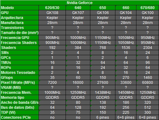
Has anyone seen these?

24yoljb.png

nvidiakepler.jpg


If these are Q4 2012 GPUs, it doesn't sound too far off, right?
Those ~1.3GHz factory overclocked HD7970 may go head to head with this GTX 770 if driver improvements are due, and that wouldn't be too far off from the HD5870->GTX470 situation, for example.
 
If these are Q4 2012 GPUs, it doesn't sound too far off, right?
Those ~1.3GHz factory overclocked HD7970 may go head to head with this GTX 770 if driver improvements are due, and that wouldn't be too far off from the HD5870->GTX470 situation, for example.

1. Those specs are random speculation, wouldn't put too much stock in it.
2. If the 7970 needs a 40% overclock to match its fabled competition that's going to be very different to 5870v470.
 
1. Those specs are random speculation, wouldn't put too much stock in it.
You may be right, but they are appearing in different sites at the same time..


2. If the 7970 needs a 40% overclock to match its fabled competition that's going to be very different to 5870v470.

40% overclock relative to what?
Factory overclocked means it wouldn't need a 40% overclock...

Besides, given the absurd overclocking potential of Tahiti we've seen so far, I wouldn't be surprised if by Q3 2012 AMD comes out with some HD7xxx "+" or "XTX" or just HD8xxx with rebranded+overclocked SI chips in order to keep competing with nVidia on the performance front.
 
Has anyone seen these?

24yoljb.png

Yeah, also did you hear pigs started flying on their own?
There's simply no way "GTX780" would be over twice as fast as GTX580 and around 50% faster than GTX590

edit:
Actually, I'm 99.99% sure that the "2304" shaders on the supposed GK100 comes from the supposed Sapphire document which showed "Tahiti with 2304 shaders" scratched

edit2:
Also, take a look at the "GFLOPS" part of the table.
 
Back
Top