NVIDIA Kepler speculation thread

Maybe as a safety net to be at least able to wage a price war if AMD is on time with 28nm next-gen and Kepler might be late? Remember the GT200 disaster end of 2009 where Nvidia stopped production of 55nm GT200 chips and had nothing to compete from lower midrange upwards.

In response to the problems with the larger GPUs, NV has changed their ramp-up cycle a bit. The smaller GPUs of the same family do no longer "wait" for the biggest to be ready.
 
In response to the problems with the larger GPUs, NV has changed their ramp-up cycle a bit. The smaller GPUs of the same family do no longer "wait" for the biggest to be ready.

And that is planned or a consequence?
 
And that is planned or a consequence?

Why do you think they had to wait in the past for the top dog to roll out in order to start rolling out smaller chips? Because it wasn't simply possible. The more problematic manufacturing processes get and since they started with 40nm again using the smallest available manufacturing process they should had laid out Fermi as Kepler in the past too.
 
neliz said:
And that is planned or a consequence?
What do you think?

Of course it is planned... Do you think these things just happen? As in: 'gee, the big one was supposed to be 3 months before the small one. And now suddenly it's the opposite!'
 
And that is planned or a consequence?

A concequence. :cool:

Why do you think they had to wait in the past for the top dog to roll out in order to start rolling out smaller chips? Because it wasn't simply possible. The more problematic manufacturing processes get and since they started with 40nm again using the smallest available manufacturing process they should had laid out Fermi as Kepler in the past too.

Wasn't it more like a strategy to offer enthusiasts what they were waiting for? One can say that those customers should get latest technology first and then the mainstream some salvage parts.
Plus, if I recall correctly, it is easier to build a big chip and then to cut it for smaller parts, than the other way round.
Now, as you also point out, if they use the same strategy, it would be a very very long wait for those smaller parts. That means more lost market share.
They simply learn from their mistakes.
 
What do you think?

Of course it is planned... Do you think these things just happen? As in: 'gee, the big one was supposed to be 3 months before the small one. And now suddenly it's the opposite!'

When the "big one" gets scrapped and replaced with another "big one" I would have to say yes these things do happen.

1. It's not late.
2. Doing Fermi shrinks on 28nm is as time consuming as doing Keplers on 28nm thus if you'd do Fermi shrinks then it'd be a given that Keplers will be late.

You friend Charlie disagrees...
http://semiaccurate.com/2011/12/01/can-nvidia-supply-apple/
 
LordEC911 said:
When the "big one" gets scrapped and replaced with another "big one" I would have to say yes these things do happen.

You friend Charlie disagrees...
http://semiaccurate.com/2011/12/01/can-nvidia-supply-apple/
Too me, it seems as if he's just writing a story based on the 4gamer leak. Which is shaky to the point if being very unbelievable. (GK110=2 chips? That'd be an Nvidia first.)

Given his bad track record, especially when it comes to anything silicon kitchen related, why would he be right this time?
 
Too me, it seems as if he's just writing a story based on the 4gamer leak. Which is shaky to the point if being very unbelievable. (GK110=2 chips? That'd be an Nvidia first.)

Given his bad track record, especially when it comes to anything silicon kitchen related, why would he be right this time?

His track record isn't very good when it comes to the technical side of things. I mean, come on: "Then again, they did spin the 28nm shrink of Fermi, something that should be somewhere between a cakewalk and a no brainer."

That said, his track record with schedules and delays is, to the best of my recollection—at the risk of sounding like Herman Cain—quite good indeed. Also, I seriously doubt he would publish something like this if his own sources didn't corroborate the 4Gamers story.
 
Last edited by a moderator:
1. It's not late.
2. Doing Fermi shrinks on 28nm is as time consuming as doing Keplers on 28nm thus if you'd do Fermi shrinks then it'd be a given that Keplers will be late.

1. We don't know yet.
2. Not if you have different teams working on it. For a proven architecture, I can imagine you'd need more engineers from the design/fab interaction branch, whereas for ramping up a new architecture as well as a new process, you'd need additional people from the design team. Besides: It can greatly help if your process of choice is ready, but you have trouble with your design.


That had much more to do with them doing GF100 first and GF104 later than not doing Tesla shrinks on 40nm (although you could say that they did do them in the form of GT21x). With Keplers it'll be different since they're doing low and mid first and high-end later.
It had much to do with Nvidia knowing AMD would have smaller, faster, more modern ASICS out there and no one would want GTX 2xx for a reasonable price anymore. If they'd been able to shrink it to half it's size, maybe then they'd had the option of at least competing price wise without making a big loss for every (high-end) GPU sold.
 
2. Not if you have different teams working on it. For a proven architecture, I can imagine you'd need more engineers from the design/fab interaction branch, whereas for ramping up a new architecture as well as a new process, you'd need additional people from the design team. Besides: It can greatly help if your process of choice is ready, but you have trouble with your design.
I don't think the architecture of the chip has much thing to do with the production as long as it is not a extremely big chip
 
http://forums.laptopvideo2go.com/topic/29042-v29518-windows-7vista-64bit-asus-mobile/

[DEV_0FDB&SUBSYS_10AC1043] NVIDIA GK107-ESP-A1

Also other SKU strings included for DEV_0FD... devices, which are rumored to be GT 640M, GT 650M and GTX 660M.

Well, since nVIDIA starts at A1, it doesnt look like they run into problems with GK107, contrary to what some people are saying. Or would they put the strings of a broken part on a driver they sent to ASUS?

EDIT - Or not. ESP can mean Engineering Sample?
 
Last edited by a moderator:
Wasn't it more like a strategy to offer enthusiasts what they were waiting for? One can say that those customers should get latest technology first and then the mainstream some salvage parts.

Wouldn't it be wiser for any IHV to adjust its roadmap according to demand and not the other way around? With Intel getting way more aggressive with its embedded graphics NV has every reason to think differently and with the global financial crisis even more so since lower end products will obviously be in a much higher demand.

On top of that newest/smallest manufacturing processes are getting constantly more problematic. It's obviously wiser to wait for foundries to iron out yields and capacities for those and produce whatever is possible at reasonable yields and in extension manufacturing costs and build up from there up to the high end. NV could have theoretically sent even it's Kepler top dog into production in fall this year; the average manufacturing cost per die would had been insane though and what's left then is to either sell chips at a healthy loss or charge uberprices for them. Would you rather pay for a high end GPU somewhere under a $1000 or would you rather wait N months and pay half as much?

Plus, if I recall correctly, it is easier to build a big chip and then to cut it for smaller parts, than the other way round.

I'd love to stand corrected but I'd say it's rather a matter how you plan N product family when you start with it (or at worst as early as possible during the development process). I have a hard time understanding why a desktop GPU can scale from top to bottom and not the other way around (always in a highly relative sense).

No IHV is actually "cutting" any chips when designing from top to bottom. While it's fairly easy to take an existing desing and tailor a smaller variant out of it, there's still a considerable amount of work involved and that's exactly the reason why high end to lower end chips don't typically launch all within the exact same time-frame.

Now, as you also point out, if they use the same strategy, it would be a very very long wait for those smaller parts. That means more lost market share.
They simply learn from their mistakes.

Exactly. In fact albeit being a layman their change of strategy is exactly what I suggested in various forums shortly after the Cypress launch for Fermi. Many suggested back then that it isn't possible; well it obviously wasn't for Fermi since it was way too late, but definitely not for succeeding generations. Albeit I could be wrong GK107 doesn't strike me as the smallest Kepler chip either.
 
I'd love to stand corrected but I'd say it's rather a matter how you plan N product family when you start with it (or at worst as early as possible during the development process). I have a hard time understanding why a desktop GPU can scale from top to bottom and not the other way around (always in a highly relative sense).

I think it's a matter on how you align your strategy with production and AMDs later VLIW5-chips (HD5k especially) and Nvidias GF1xx generation showed much of the pros and cons to both approaches.

Nvidia had a little more complete processors as building blocks (SIMDs) which were necessary to allow the very good scaling to an enthusiast level GPU and high performance computing that Nvidia needed. But at the same time they were also larger than the competitions' thus loosing their edge more and more the lower scaled the corresponding ASICs became. AMD on the other hand optimized the area-and-power-hell out of their SIMDs as they are but had to accept that on normal/general workloads the scaling with increased number of SIMDs was worse than the competitions and a lot of their on-paper-advantage in terms of throughput, peak performance etc. vanished when applied to normal/regular workloads.

GPUs IMO can scale either way, but going top to bottom you'll have more effort up front, but you're probably more inclined to optimize your building blocks more toward better scaling with higher unit counts paying the price in area and performance. Going the other direction could lead to a dead end street when you realize that just adding more units won't return on your investment any more, even if you've got ample headroom in power and die space left.
 
Last edited by a moderator:
There is scaling in the design and in production. I see no reason why you could not do a top-down scaling in design, but do the reverse in production.

Every chip needs its own tape-out anyway. We do not even know, if both IHVs might not even had tape-outs of the big chip or even the whole line. Based on the success (or lack of) of the 28nm process in mass production, they could add one SKU after the other depending on the improvements of yield and general maturity of the process. If GK107 is the second smallest SKU, it might be a good chip to put into production first. Then you do GK104 and finally the top-dog and the smallest chip, when the process is mature and the wafers have become cheaper.

GK107 is a good start, a limited production efficiency would still sell well in the mobile sector, if you have improved the power consumption. Then you go GK104 which is the mobile topdog and the performance chip in the desktop market.

And the best of it. You can easily adjust the price based on improving yields of GK107, when GK104 comes and you can do it again for GK104 when GK110 (or whatever the big chip is called) arrives.
 
From what he's saying there I can conclude that Charlie just doesn't know anything about Kepler.

1. We don't know yet.
Right.

2. Not if you have different teams working on it. For a proven architecture, I can imagine you'd need more engineers from the design/fab interaction branch, whereas for ramping up a new architecture as well as a new process, you'd need additional people from the design team. Besides: It can greatly help if your process of choice is ready, but you have trouble with your design.
Now where would you get another team for this? Anyway, all the leaks up till now point to some GF119 being the only Fermi on 28nm and it's all GKs after that. Having GK107 in the drivers is pretty much a confirmation that we won't get any GF on 28nm higher than that.

It had much to do with Nvidia knowing AMD would have smaller, faster, more modern ASICS out there and no one would want GTX 2xx for a reasonable price anymore. If they'd been able to shrink it to half it's size, maybe then they'd had the option of at least competing price wise without making a big loss for every (high-end) GPU sold.
GF100 was supposed to launch in the end of 2009 alongside Cypress. A shrink of GT200 would be able to compete with Juniper but not Cypress. Thus any Tesla-generation shrunk to 40G would not be able to compete with new AMD's offerings. And that's exactly the point why there is zero reason to shrink Fermi to 28HP now - in the same fashion none of Fermi chips even at 28nm would be able to keep up with Tahiti. Doing a Fermi architecture chip bigger than GF110 for 28nm is counter productive when you have a whole Kepler line-up (which is much more than just Fermi shrunk to 28nm really) for that. The lesson NV learned from GF100 is not that you should do a "safe" shrink first to have "something" to compete against AMD, it's that you should first do a chip which is destined to compete with what AMD is doing first, not some big HPC-driven power house which AMD won't ever have a part against. And that's why we'll see GK107, 106 and 104 first and 110 later.
 
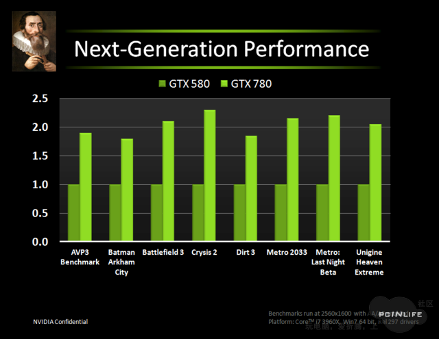
0908157p020sn1srmmmklq63b2.png


http://we.pcinlife.com/thread-1802355-1-1.html
 
Back
Top