I thought it's 64bit so not quite that bad. Maybe at least for the 32 ALU SMs it is "enough".
Yes, sorry 64-bit. Theoretically for any non-trivial shader it's enough but it seems rather tight.
Follow along with the video below to see how to install our site as a web app on your home screen.
Note: This feature may not be available in some browsers.
I thought it's 64bit so not quite that bad. Maybe at least for the 32 ALU SMs it is "enough".
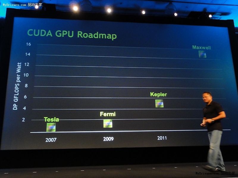
Most definitely, 2 years is enough time to implement it. Its possible NV knew about this technology for a while now.Are we going to see this used in Maxwell?
http://www.xbitlabs.com/news/cpu/di..._for_Heterogeneous_Multi_Core_Processors.html
Yes, that's what I wanted to say, the GF104 SMs don't look that much more efficient now, and if you'd extend them for faster FP64 they might not really have that much of an advantage.
Well that those SMs can't be at peak rate with only 40 instructions per shader follows directly from the 64bit per clock export alone (there could well be other reasons too). With 40 instructions there will be 48/40 pixels per clock at peak rate, which is 1.2 pixels / clock. But that's at hot clock, at normal clock that's already 2.4 pixels per clock - 20% over the 2 pixels (64bit) / clock limit. So because of that alone you'd need at least 48 instructions to reach peak efficiency (and 32 instructions for GF100/GF110).From what I saw they mostly look pretty weak, the shorter the shaders are - which seems to be the case quite often in synthetic programs trying to measure maximum throughput.
A small but practical question: when is exactly Kepler expected to be released? Will be ready for BF3 (October, 25) or are we sailing in the November-December timeline?
The next GTC is May 2012. They're skipping 2011 entirely and that could be because they have nothing to show as yet.
Wow, I didn't know that… That's not a very good sign. I sure hope they can manage to release something before May 2012, especially if AMD succeeds in launching Southern Islands this year in 28nm, or it's going to be HD 5870 vs GTX 285 all over again.
")
Interesting paper by Lindholm and Dally. Lindholm designed G80's shader core and Dally is nVidia's current chief architect so this stuff could show up in future architectures. The goal is to reduce power consumption by simplifying the scheduler and register file access.
First bit focuses on creating a two-level scheduler hierarchy. The first level holds all warps including those waiting for long latency instructions (texture and global mem fetches). The second level contains only 6-8 active threads. An active thread is one that's executing or waiting on a low latency instruction (ALU or shared memory fetches). All instruction issue happens from the small active pool and threads are swapped between pools as necessary.
The second complementary piece is register file caching. According to the paper the register file consumes 10% of chip dynamic power consumption and a single access uses more power than an FMA. The idea is to cache 6 registers per thread in a small multi-ported register file with single cycle access to all operands. So no need for an operand collector and the register cache can be located nearer to the ALUs. Only the registers from active threads are cached. Flushes to the main register file are required if a thread gets evicted from the active pool. Compiler hints help reduce flushes by marking registers as dead after their last reference in the instruction stream.
All this work for a grand total of 3.6% reduction in power consumption plus an increase in power consumption due to register cache flushes.
http://cva.stanford.edu/publications/2011/gebhart-isca-2011.pdf
What is a bit funny, is that half of their reduced number of reads of the main register file are actually reads of results of the immediately preceding instruction. AMD' VLIW designs catched those compeletely with their pipeline register PV and PS (and they even managed to use that for reducing the instruction latency, opposed to the proposed solution in the paper).
That's why they recuded register file size per ALU, at least according to them.When I think about it, Fermi also reduced latency already compared to earlier design.
I would think that with proper result forwarding and pipelined register reads not contributing to the instruction latency (as in CPUs) it is very possible to get a 4 cycle latencyDo you reckon that would still be possible in Southern Islands?
You are right, I only skimmed through the paper and mixed up a few numbers in that course. And the 50% reuse is what nvidia gets from their modelling, I was only saying one could get half of it almost for free.However the savings are also much smaller; I'm not sure where you're getting the idea you can get 50% of the reuse with it as Figure 6 clearly says otherwise.
But higher latency means a tendency towards more necessary active warps from which a need for a higher capacity of the inner scheduler and also a larger RFC would result. So a shorter latency would increase the possible benefits.Also this does not limit NVIDIA to an artificially low number of ALU pipeline stages. The inner scheduler is said to be capable of hiding shared memory latency on its own, which is 20 cycles in the paper. Remember that the inner scheduler is greedy and not round-robin.