Install the app
How to install the app on iOS
Follow along with the video below to see how to install our site as a web app on your home screen.
Note: This feature may not be available in some browsers.
You are using an out of date browser. It may not display this or other websites correctly.
You should upgrade or use an alternative browser.
You should upgrade or use an alternative browser.
NVIDIA GF100 & Friends speculation
- Thread starter Arty
- Start date
I'm guessing these are DP-castrated as well. The test doesn't really make it clear.
From neliz's linked pdf. IIRC the 8x number was for DP. But in general most of the Quadro marketing seems laser focused on geometry. Guess they can't eat too much of Tesla's lunch.
Modern applications harness the latest NVIDIA® CUDA™ parallel processing architecture of Quadro GPU to deliver performance gains up to 8x faster compared to previous generations when running computationally intensive applications such as ray tracing, video rocessing and computational fluid dynamics
Well, if you think about it, for cluster GPGPU computing applications, in some instances these cards may be worth it.
But Quadro is not really meant for clusters, is it?
The new Quadros are 1/2 DP-rate. That was made pretty clear by Nvidia.
http://translate.google.de/translat...ermi-Innenleben/Grafikkarte/News/&sl=de&tl=en
http://translate.google.de/translat...ermi-Innenleben/Grafikkarte/News/&sl=de&tl=en
Hmmm, perhaps. I guess I was working under the assumption that these were the same cards as Tesla, with Tesla just being the cards put into systems. Could be wrong, I suppose.But Quadro is not really meant for clusters, is it?

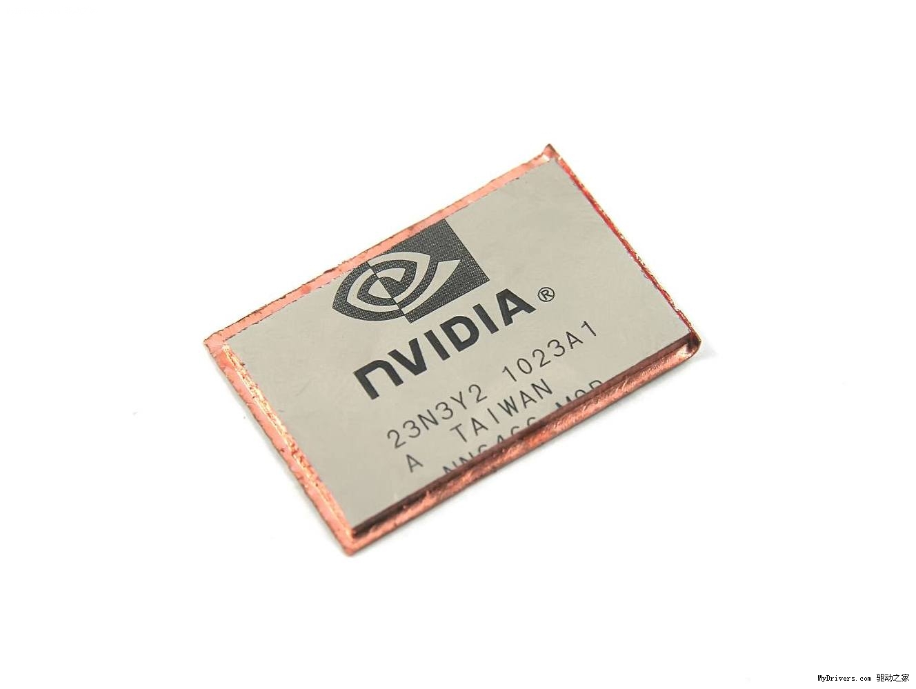
Thanks for posting. And interesting, if those measurements are true, since Charlie confirmed the die size to be 367 mm². Two versions of GF104? The pictured one apparently comes from the cut-down version with one ROP partition disabled.
Thanks for posting. And interesting, if those measurements are true, since Charlie confirmed the die size to be 367 mm². Two versions of GF104? The pictured one apparently comes from the cut-down version with one ROP partition disabled.
Could I have whatever you're smoking, please?

As for the measurements, anyone got the packaging measurements for other places for comparison to see if they're correct?
Much more insanity than that:Wow!
Is the cap sanded down? Pretty clean work.
http://news.mydrivers.com/1/171/171023.htm
Could I have whatever you're smoking, please?
 Maybe it would be easier to say: "If this measurements are more than semi accurate, Charlie seems to have been wrong."
I know, wasn't being serious
Hmm 13.7 x 24.2.its around ~332mm^2
According to Charlie it is 14.7 x 24.9.
Looks like some quite big measurement error somewhere to me...
Silent_Buddha
Legend
Measurements for that picture are incorrect.
Either the inner die measurements are wrong or the outer shim measurements are wrong. According to the measurements in the pictures the short side of the outer shim should be ~2.45x the short side of the die, yet if you do even a rough measure of the picture is much less than that coming in at ~2.33x.
Evidently someone either doesn't know how to measure or are being deliberately misleading.
If someone has measurements for the actual outer shim, you should be able to get a fairly good estimate of the die measurements.
Regards,
SB
Yeah, something is wrong.
If we go by the outer measures on the pic, we'll get 24.7*14.1 mm
Where do those numbers in this post actually come from? the linked picture is without the measurements, so apart from being inconsistent (maybe not taking the perspective distortion into account), what known measure is it based on?
Anyone with a good hires naked board pic? I prefer using the 89mm pcie connector as base..
If I use This picture and a coin size of 24.26mm (wikipedia), I get the white rounded square around the chip to 49.5*39.1mm, and putting those numbers into this I get a chip size of 25.2*14.5 = 366mm2 (...)
Last edited by a moderator:
Much more insanity than that:
http://news.mydrivers.com/1/171/171023.htm
*chuckle*
The pic isn't face-on. Could just be a perspective issue.Measurements for that picture are incorrect.
Most probably it is as simple like this.The pic isn't face-on. Could just be a perspective issue.
I wouldn't trust measurements from such shots, as you can have a 5% margin of error for each side easily.
Perspective aren't that much of of problem (picture is taken with 70mm zoom btw), as long as you take the right measures.
His numbers are clearly inconsistent, and we don't know which absolute measure it's based on. Does the version with the numbers even come from the same place as the picture?
Here you go regarding proportions, error should be more like 0.5%

His numbers are clearly inconsistent, and we don't know which absolute measure it's based on. Does the version with the numbers even come from the same place as the picture?
Here you go regarding proportions, error should be more like 0.5%
Last edited by a moderator:
Similar threads
- Replies
- 6
- Views
- 424
- Replies
- 14
- Views
- 3K
- Replies
- 5
- Views
- 764
- Replies
- 166
- Views
- 11K