NVIDIA discussion [2024]

  • Thread starter Deleted member 2197
  • Start date
That’s not how prices are determined. At best costs create a floor for minimum pricing. They definitely do not determine maximum pricing. Competition and consumer demand drives that. The average person has zero idea what the manufacturer is “getting out of the chip” and it’s not part of the value proposition.

We’re not buying tiers or brand names. Your entire framework for thinking about this is based on immaterial attributes of the product.
I already said that. Forget about the damn pricing for a second. These cards... and all generations of cards.. are separated into tier ranges by Nvidia and AMD. There's acceptable price ranges for each tier of card.

Nah, It's entirely based off what value Nvidia thinks these tiers are worth relative to each other.
 
It must really piss off the "official" keynotes. Keynotes fighting for view clicks ... :LOL:
Though makes sense since Nvidia has an AI Summit on June 5 in Taipei.
 
Last edited by a moderator:
It must really piss off the "official" keynotes. Keynotes fighting for view clicks ... :LOL:
Though makes sense since Nvidia has an AI Summit on June 5 in Taipei.

You think so? Nvidia probably won’t announce anything new after their big splash at GTC. All eyes will be on Lisa.
 
You think so? Nvidia probably won’t announce anything new after their big splash at GTC. All eyes will be on Lisa.
Yeah, people are wondering about their AI products. Lack of MLPerf participation by AMD or any partners has generated speculation regarding the product.
Intel will likely draw interest and benefit from their participation in the benchmark.
 
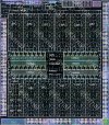
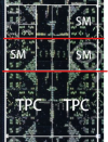
If accurate then about 1/3 of each TPC is allocated to something besides the SMs. Polymorph engine perhaps? With the GPC level rasterizers & ROPs that’s a lot of silicon dedicated to 3D fixed function.

This should probably be in the architecture thread though.
 
We don't know that really and we don't know why the SMs are marked as they are above either. In Nvidia's logical schemes there are nothing but 2 SMs in 1 TPC.

Look at the symmetry. That unmarked block is 1 per TPC. So likely not SM specific. We know that each SM has dedicated cache and LDS.

Also that block looks far too large to be the relatively small SM L1 (compared to the size of the 2M L2 slices).
 
Look at the symmetry. That unmarked block is 1 per TPC. So likely not SM specific. We know that each SM has dedicated cache and LDS.
A TPC can be horizontal instead of vertical as drawn above. In that case that central area would divide between 2 SMs in a pretty symmetrical fashion.

1714375484704.png
 
Where? Seems about as symmetrical as when cut vertically. This way you're dividing the central area between both SMs and TPCs though which is what the layout suggests.

With your cut that central area is no longer symmetrical across TPCs. Either way it’s too large to be 128KB cache. My guess is it’s fixed function bits. With mesh shaders becoming a thing and triangle counts increasing it probably makes sense to keep the FF triangle setup stuff but Nvidia seems to have a lot of it and it’s not clear how much it helps in real workloads.
 
I don’t think we “know” exactly what is in the SM vs TPC - e.g. based on my testing, I am fairly confident the L0 instruction caches are per-multiprocessor, the L1 instruction caches are per-TPC (32KiB, used to be 12KiB on Volta) and the L1.5 instruction/constant caches (128KiB) are per GPC. But that’s not what either NVIDIA claims in their diagrams (L1 instruction cache per SM) or what the Volta dissected paper (which is really good but far from its only mistake).

A 32KiB cache isn’t going to take anywhere near that much area but it’s just to illustrate we don’t really know.

The fact that area is very RAM-light implies it might have a large percentage of wire-heavy/wire-only areas for communication to the L2 and GPC central area as well.
 
I don’t think we “know” exactly what is in the SM vs TPC.

No we don’t but we can make some informed guesses based on per-TPC and per-SM resources. E.g. Nvidia has claimed each TPC has triangle setup, tessellation hardware etc so that’s gotta be in there somewhere.
 
No we don’t but we can make some informed guesses based on per-TPC and per-SM resources. E.g. Nvidia has claimed each TPC has triangle setup, tessellation hardware etc so that’s gotta be in there somewhere.
Yep absolutely, that sets a minimum of what is in there, just there’s probably more than we know - e.g. if raytracing was mostly per-SM but shared a bit of logic per-TPC, how could we possibly know that? These kind of implementation details really aren’t relevant for marketing material.

What would be interesting is a H100 die shot if they did indeed turn out to remove graphics logic from most SMs/GPCs like they implied they did, but I’m not sure whether that’s completely true.

BTW Fritzchens Fritz already had an AD102 die shot for a while, but no public H100 ones that I know of or have ever seen :(
 
Back
Top