Nvidia Ampere Discussion [2020-05-14]

a100knjxq.jpg

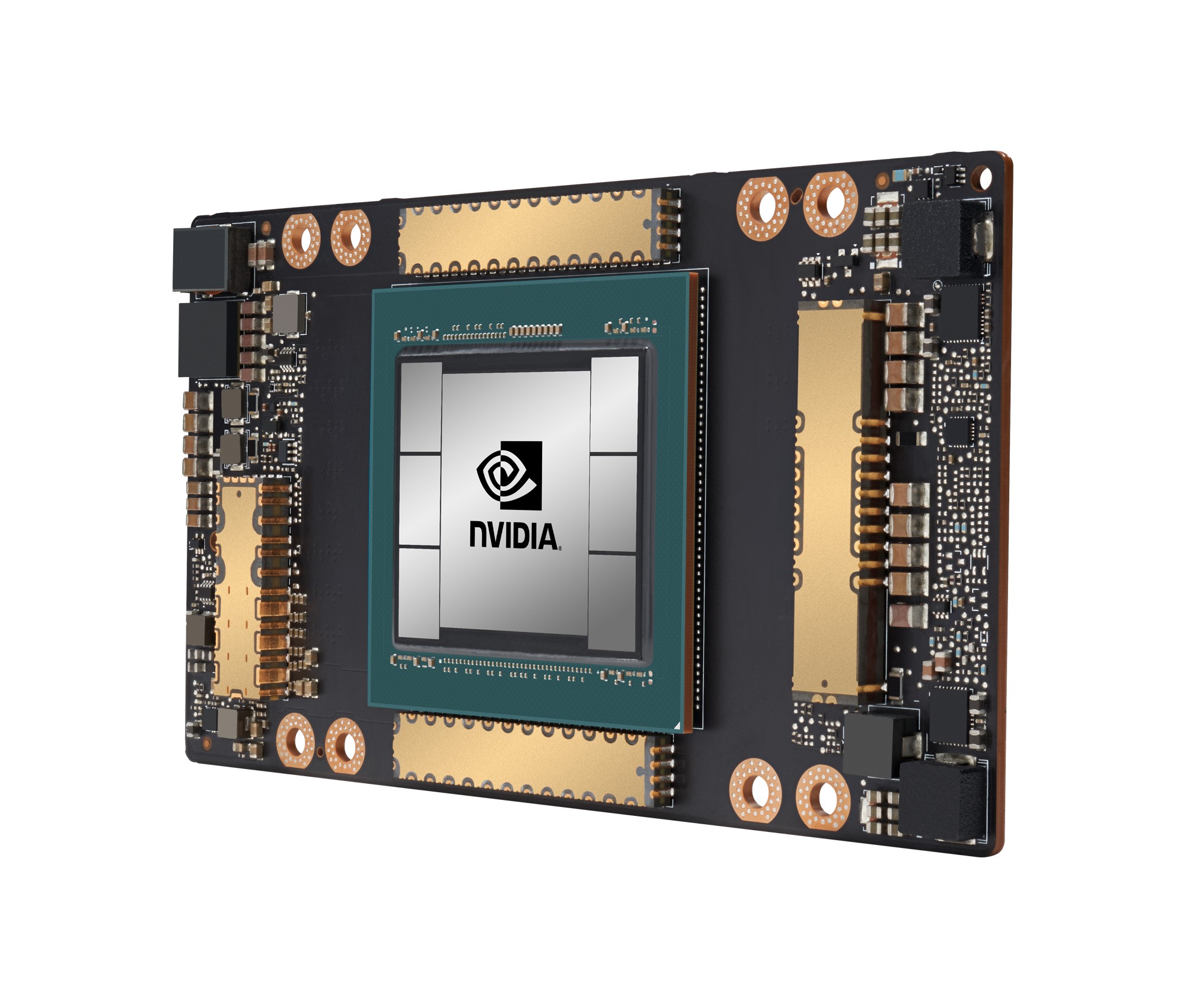
A100 SXM2
I found the die size around 806mm2

Edit: EETimes went ahead and published the article before its due

Nvidia Reinvents GPU, Blows Previous Generation Out of the Water
The first chip built on Ampere, the A100, has some pretty impressive vital statistics. Powered by 54 billion transistors, it’s the world’s largest 7nm chip, according to Nvidia, delivering more than one Peta-operations per second. Nvidia claims the A100 has 20x the performance of the equivalent Volta device for both AI training (single precision, 32-bit floating point numbers) and AI inference (8-bit integer numbers). The same device used for high-performance scientific computing can beat Volta’s performance by 2.5x (for double precision, 64-bit numbers).
[...]
The Tensor Cores now also natively support double-precision (FP64) numbers, which more than doubles performance for HPC applications.
[...]

http://archive.is/fiMX1
 
Last edited:
The Ampere GA100 GPU ... to pack 128 SM units, equalling a total of 8192 CUDA cores... For memory, we are looking at six HBM stacks that point out a 6144-bit bus interface. The memory dies are definitely from Samsung who has been NVIDIA's strategic memory partner for HPC-centric GPUs.
Finally, NVIDIA will be announcing its next-generation DGX-A100 system which Jensen Huang teased a few days ago. The DGX-A100 will deliver 5 Petaflops of peak performance with its 8 Ampere based Tesla A100 GPUs. The system itself is 20x faster than the previous DGX based on NVIDIA's Volta GPU architecture. The reference cluster design features 140 DGX-A100 GPUs with a 200 Gbps Mellanox Infiniband interconnect. The whole system is going to start at $199,000 and is shipping as of today.
NVIDIA also confirmed that the DGX A100 systems are already in operation in the US Department of Energy (Aragone National laboratory), where they are used to fight Covid-19.

PS:
A reference design for a cluster of 140 DGX-A100 systems with Mellanox HDR 200Gbps InfiniBand interconnects, the DGX-superPOD, can achieve 700 petaflops for AI workloads. Nvidia has built a DGX-superPOD as part of its own Saturn-V supercomputer, and the system was stood up from scratch within three weeks. Saturn-V now has nearly 5 exaflops of AI compute, making it the fastest AI supercomputer in the world.
For Jensen personal usage :runaway::runaway::runaway:
 
Last edited:
"Nvidia claims the A100 has 20x the performance of the equivalent Volta device for both AI training (single precision, 32-bit floating point numbers) and AI inference (8-bit integer numbers)." ....if you use new Tensor Float 32 -precision not supported by Volta
 
Regarding the demo, we've had it heavily implied (possibly stated directly) that it runs on both XSX and PC so it's probably a little premature to start claiming it's only possible because of the PS5's SSD.

That UE5 demo is probably even more impressive compared to what NV can tech demo on a 3080/nvme optane system.
 

it's a change from previous Volta / Turing gen

another source:
https://www.marketwatch.com/story/n...is-coronavirus-2020-05-14?link=MW_latest_news
Ampere will eventually replace Nvidia’s Turing and Volta chips with a single platform that streamlines Nvidia's GPU lineup, Huang said in a pre-briefing with media members Wednesday. While consumers largely know Nvidia for its videogame hardware, the first launches with Ampere are aimed at AI needs in the cloud and for research.

“Unquestionably, it’s the first time that we’ve unified the acceleration workload of the entire data center into one single platform,” Huang said.


Nvidia discovered years ago that its gaming hardware was beneficial to machine learning thanks to its parallel-processing design — when researchers attempt to “teach” algorithms with data, GPUs help to push more of that data through at a faster rate. It has steadily developed products based on those needs for high-performance computing, data centers and autonomous driving since.
 
Last edited:
So now that Ampere is the overall arch for consumer and HPC, consumer chips will most likely cut down on Tensor units count, there is also a possibility of a Titan Ampere GPU as well, like Titan V.

The bigAmpere HPC is definitely a 128SM GPU, we need to figure out the frequency and power consumption now so we can infer some info about the rest of the lineup.
To reach 5PTFLOPS it needs a bit more than 128SM. Or really high clocks.
 
8 GPUs pushing 5 PFLOPS is around 625 TFLOPS per GPU, clearly they're talking about Tensor-FLOPS and not general FP32 FLOPS

Yeah I was being very lazy on the maths. This sounds correctto me then as the 2080Ti is rated at 440 TFLOPS in INT4 and that's with 80SM's. So it seems to be running at a slightly slower clock than the 2080Ti all else being equal.
 
So NVIDIA effectively traded FP32 CUDA cores with FP32 Tensor Cores, Tesla A100 is really just Ampere optimized for AI.

Regular FP32 is : 19.5 TF
Tensor FP32: 156 TF, accelerated to 312 TF effective through "sparse acceleration"

Consumer Ampere will definitely cut down on the advanced tensor stuff and trade back the lost FP32 CUDA cores.
 
Last edited:
Back
Top