Next Generation Hardware Speculation with a Technical Spin [pre E3 2019]

Status
Not open for further replies.
More food for thought: AMD's GPU development history

AMD's Top-end Single GPU Video Card
2012 - 7970 - 28nm - 3.79 TF
2013 - R9 290X - 28nm - 5.63 TF
2015 - Fury X - 28nm - 8.6 TF
2017 - Vega 64 (Air) @ Boost Clock - 14nm - 12.67 TF
2019 - Radeon VII @ Boost Clock - 7nm - 13.82 TF

Consoles based on AMD GPU
2013 - PS4 - 28nm -1.8 TF
2016 - PS4 Pro - 14nm - 4.2 TF
2017 - Xbox One X - 14nm - 6 TF

A console based on a SoC containing an AMD GPU has never had more than 1/2 the total TF capability of the top-end GPU from AMD at any time during this period. Keep that in mind when setting your expectations for the performance of next-gen consoles.

Perhaps we should be looking at the power consumption figures to get a better sense of the limitations as well as the die size. Might also be worth gauging the relative clock speeds as well vs the sustained-under-load clocks on desktop.
 
Perhaps we should be looking at the power consumption figures to get a better sense of the limitations as well as the die size. Might also be worth gauging the relative clock speeds as well vs the sustained-under-load clocks on desktop.

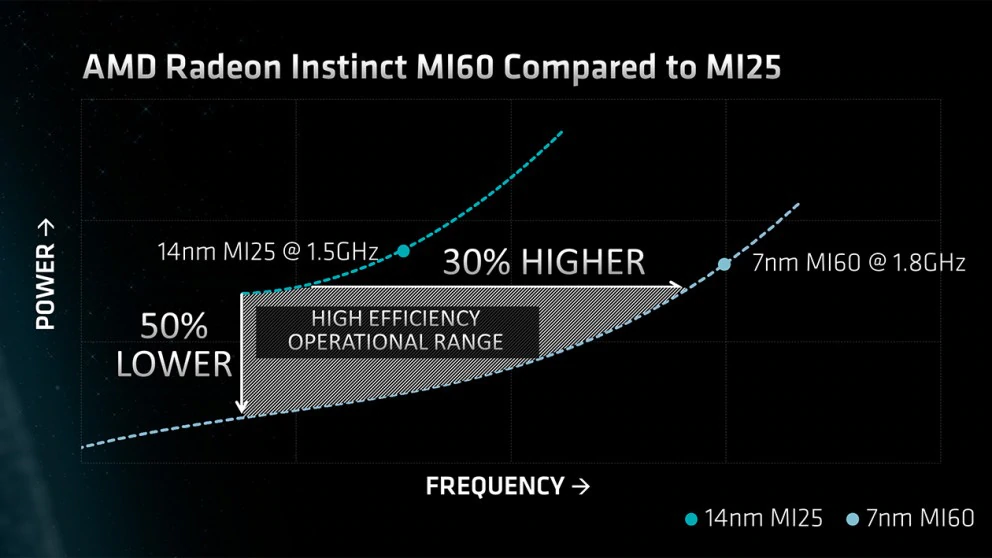
Precisely. AMD’s own data says they can maintain performance level at half the power going to 7nm. So you have a 331mm^2 die at at 12TF and 150W with extra die space dedicated to a larger than needed memory bus, INT8/4, and FP64 that you don’t need for gaming tasks.

InstinctMI60MI25.png
 

haha holy shit I hadn't seen it I swear. I got the idea from seeing the die size of the Vega VII today but looks like that number was already out there with the MI60 anyway...

I think if it can fit ~56CU's then that means we are probably looking at 52 active CU's.

Also I suspect they will match or better Xbox One X's 1172Mhz clock...if they manage to get to 1.5GHz that would give them pretty much 10Tflops....which would be nice from a marketing standpoint...and god knows Microsoft loves that.

Of course this CU math assumes Micrososft is targeting a ~360mm^2 die size. It's possible they just go bigger.
 
They "gave up the PC GPU battle" if they don't support, at launch, a feature that is currently implemented in one (1) title with a huge performance hit and very questionable IQ enhancements?

Turing is one of the most impressive launches to me, being able to run 60fps at highest settings and highest DXR settings in BFV isnt anything bad. Also not just one title, and more will follow.

https://www.forbes.com/sites/marcoc...mes-that-will-support-nvidias-rtx-technology/

Yea lol.
Given the price points we are working with I’m often baffled at the call for 10+ TF as being reasonable.

Newer features will define the generation not power output. Variable rate shading, mesh shaders/primitive, GPU side draw calls, RT, ML res, animation, physics and denoising. Etc etc.

6-7TF with this feature set is going to drive much larger gains in image quality and performance than simply more flops.

That being said, without a doubt they will cram in as much power as they can, but should not do so at the cost of these new features.

People tend to go for numbers. Nothing wrong with dreaming though :)
 
Turing is one of the most impressive launches to me, being able to run 60fps at highest settings and highest DXR settings in BFV isnt anything bad. Also not just one title, and more will follow.

I agree that it's not a bad thing, but don't you think the RTX2080 being able to run BFV at its highest DXR settings is more to do with the RTX2080 being the targeted GPU, on account of it being the ray tracing GPU?
 
haha holy shit I hadn't seen it I swear. I got the idea from seeing the die size of the Vega VII today but looks like that number was already out there with the MI60 anyway...

I think if it can fit ~56CU's then that means we are probably looking at 52 active CU's.

Also I suspect they will match or better Xbox One X's 1172Mhz clock...if they manage to get to 1.5GHz that would give them pretty much 10Tflops....which would be nice from a marketing standpoint...and god knows Microsoft loves that.

Of course this CU math assumes Micrososft is targeting a ~360mm^2 die size. It's possible they just go bigger.

I had some counter arguments in the other thread, I'm not going to copy paste them, but I will repeat that Vega 7 is not a good base for these calculations. It has too much baggage compared to a true gaming only design and is a shrink from the old 14nm process. TSMCs 7nm should offer close to 3x the amount of transistors per mm2 compared to their 16nm process, which is quite similar to the Glofo 14nm. While I'm not quite expecting that type of increase in transistors, the math that there is enough room for 56CUs when when the Xbox One X already has 44 on chip on 16nm is quite flawed imo.

having said that there could be other reasons why the CU-count might not get a large increase over the X. Higher clocks with smaller size is perhaps the best choice and cost effective, AMD architecture might have hard limit on CU-count, power scaling puts an limit there anyway or Navi CUs are physically a lot bigger?

We don't know much about Navi and the architectural improvements AMD has able to come up with it plays a critical role in how powerful the next gen consoles can be, at this point the error margin is very large.
 
I'm actually not too clear on the inutility of even lower precision for rendering, but the cost of implementing it might not be that much more.
Perhaps not, but the crux is they added 700 million transistors and probably don’t need most of them for gaming tasks.
 
Perhaps not, but the crux is they added 700 million transistors and probably don’t need most of them for gaming tasks.
Between Vega 10 and 20, yes, they added another 700M, but the addition of INT8/4 wasn't the only change. They moved to half-rate DP instead of 1/16th, doubled the ROPs, potentially added more L2 cache...
 
Last edited:
Between Vega 10 and 20, yes, they added another 700M, but the addition of INT8/4 wasn't the only change. They moved to half-rate DP instead of 1/16th, doubled the ROPs, potentially added more L2 cache...
Agreed. My point was they don’t need DP at all and the 4096 HBM2 interface is overkill.
 
I'm actually not too clear on the inutility of even lower precision for rendering, but the cost of implementing it might not be that much more.
That kind of granularity is of little use for code that does not take it in mind, but having it available means opportunity for optimization. If we were talking about offline rendering, sure, that's not worth the trouble, but in real time, graphic programers always find ways to make every last bit count. I say give them the space to shave off every bit of data they can, and eventually they will do it.
 
Probably not. FP32 gives a pretty big range to avoid artifacts or banding issues for probably the 99.9% of games. It might have to be on the scale of some NASA project before folks would notice issues with FP32 (or maybe even Star Citizen? :p No Man's Sky probably just works around it, but I haven't played either).

As milk mentions, devs may take a more serious look at what they can do with lower precision since they have higher throughput rates than FP32 on recent HW, although I'm sure they'll run into different bottlenecks than ALU throughput per se (i.e. registers, everything cache, bandwidth).

edit:

Wonder if maybe INT8/4 can be applicable to RT workloads :?: Cache will be important for the future at any rate.
 
Last edited:
Wonder if maybe INT8/4 can be applicable to RT workloads :?:
I'm struggling to see how. It'd have to be some super duper memory structure something-or-other traversal uber-tech (hope that technical terminology doesn't go too far over your head. :-|)
 
As milk mentions, devs may take a more serious look at what they can do with lower precision since they have higher throughput rates than FP32 on recent HW, although I'm sure they'll run into different bottlenecks than ALU throughput per se (i.e. registers, everything cache, bandwidth).

I would have guessed halving the size of your data can improve register/bandwith use and cache hits just as well as ALU throughput. But that, of course, depends on how smart their implementation is.
 
Its memory controller is also likely to be smaller than a 4 stack HBM2 controller.
extra die space dedicated to a larger than needed memory bus, INT8/4, and FP64 that you don’t need for gaming tasks.
they added another 700M, but the addition of INT8/4 wasn't the only change. They moved to half-rate DP instead of 1/16th
The 700M budget was most likely spent on additional memory controller logic and/or L2 caches. We know from the Vega white paper and the Vega ISA document that HBCC (i.e. the memory controller) is connected to CUs with Infinity Fabric crossbar, so this should be straightforward.

As for FP64 and INT8/INT4, this is not really new. NGU has configurable double precision rate, though 1/2th rate has been traditionally limited to professional products until now. Some INT8 ops were in Vega whitepaper and ISA document, so adding more of them would only require microcode tweaks, if their integer multiply-accumulator blocks are standard 4-bit with carry.
 
Last edited:
The 700M budget was most likely spent on additional memory controller logic and/or L2 caches. We know from the Vega white paper and the Vega ISA document that HBCC (i.e. the memory controller) is connected to CUs with Infinity Fabric crossbar, so this should be straightforward.

As for FP64 and INT8/INT4, this is not really new. NGU has configurable double precision rate, though 1/2th rate has been traditionally limited to professional products until now. Some INT8 ops were in Vega whitepaper and ISA document, so adding more of them would only require microcode tweaks, if their integer multiply-accumulator blocks are standard 4-bit with carry.
GCN and (N)CUs have the capabilities for it as architecture, but it needs more transistors than the (N)CU they use in most chips. Last AMD chip to sport 1:2 capability before Vega 20 was actually Hawaii.
 
Do we have any comparative die shots of GDDR6 vs. HBM2 controllers on the same process? Turing on 12nm and Vega on 14nm is the closest I can think to compare. I am curious how much die space they occupy comparatively. RX 590 on 12nm would be another good comparison for growth from GDDR5 to GDDR6, but I don't think there are any die shots of it out there.
 
Do we have any comparative die shots of GDDR6 vs. HBM2 controllers on the same process? Turing on 12nm and Vega on 14nm is the closest I can think to compare. I am curious how much die space they occupy comparatively. RX 590 on 12nm would be another good comparison for growth from GDDR5 to GDDR6, but I don't think there are any die shots of it out there.

Volta is 12nm with HBM2.
 
Status
Not open for further replies.
Back
Top