NEC Electronics on Xenos (downspec in dice interconnect bandwidth?)

one

Unruly Member
Veteran
http://techon.nikkeibp.co.jp/article/NEWS/20051005/109392/?ST=lsi (requires free reg)

Nikkei Tech-on has an article about the exibition by NEC Electronics at PROTEC JAPAN 2005 which was held along with CEATEC JAPAN 2005 at the same venue from Oct. 5. The short article features Xenos.
article said:
NEC Electronics exhibited the SiP (System in Package) developed for Microsoft Xbox 360 next-generation home game console at PROTEC JAPAN 2005 at Makuhari Messe from 2005/10/5.

It contains a DRAM-embedded LSI made by NEC Electronics and a graphics LSI made by TSMC in Taiwan in one package. Those bare LSI chips are laid horizontally in a package. Specifically, the graphics LSI and the DRAM-embedded LSI are connected to interposers in a package with flip chips. The reason why NEC Electronics adopted flip chip to connect them is to improve the data transfer speed between chips. In Xbox 360, the maximum data transfer speed required between the DRAM-embedded LSI and the graphics LSI is rather high at 22.4GB/sec. According to NEC Electronics, to achieve this transfer speed, they passed up wire-bonding which is popular for in-package wiring as wire-bonding results in too big wiring inductance. The work for making them in SiP is done by Microsoft.
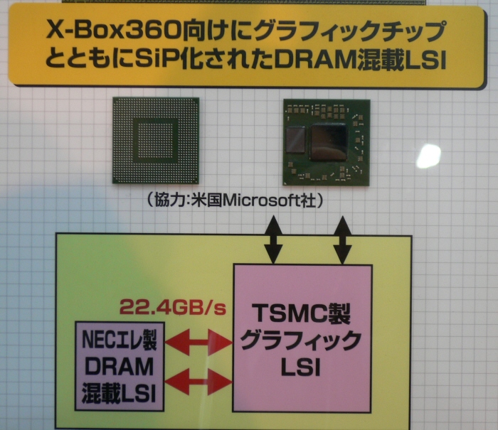
The article was published at Oct. 5 and when I first saw it I thought it's an error though the picture of the material provided by NEC clearly says it's 22.4GB/sec, not 32GB/s. Then later, a correction was added to the article,
correction said:
Though we first wrote "The work for making them in SiP is done by NEC" in this article by an interview at the event, we were informed by NEC Electronics that it's actually done by Microsoft. The article was changed according to this information.
So apparently NEC reviewed the article after it's published but the 22.4GB/sec figure stayed unchanged.

Though 22.4GB/s looks enough already, is there any impact of this downspec on game development? Another possible theory is it's just the figure for beta kit which is synchronized to a lower frequency of GPU, but I don't know the exact clockspeed of Xenon beta kit GPU, does anyone know details about this?

20051005protecfig1.jpg
 
I'm inclined to believe this is an error. 22.4 GB/s is the same speed as the DDR memory. You're bolded text reads 'transfered speed REQUIRED is 22.4 GB/s' and not 'the transfer speed IS 22.4 GB/s'. If the interconnect is handled by Microsoft and not NEC, NEC won't have their own figures for this BW. At least the PR frontmen won't necessarily. From 45 GB/s to 22.4, a figure that exactly maches RAM speed, seems very unlikely.
 
Definitely looks like a typo to me. I don't think the interconnect could be downgraded by 33% and the only thing we'd hear about it was in the form of some slide from NEC... Of course I could be wrong, but my gut instinct tells me it's not likely. :)
 
a typo in a billboard?.....
in a website publication i would understand, but in a billboard (designed and then printed) i dont think so
 
Wouldn't that mean that Xenos is running at a much lower clock than previouslly thought? But that doesn't make sense, this whole thing doesn't make sense, Ms is already manufacturing these things and nobody talked about that, not even Devs.
 
It has 2 arrows going both ways... are they indicating 22.4GB/s * 2 ?

This is a really odd picture due to the block diagram, Dave's article, and everything else available indicates otherwise.

Even more odd is the 22.4GB/s is the same as the main memory (and very similar to the FSB is I am remember right)... hmmm...
 
What's the problem?


In Xbox 360, the maximum data transfer speed required between the DRAM-embedded LSI and the graphics LSI is rather high at 22.4GB/sec.

This says the bandwidth between the Embedded DRAM and the GDDR3 is 22.4GB/s. That should be right, since 22.4GB/sec is the maximum bandwidth of the GDDR3. Obviously if that is the maximum bandwidth of the DGGR3, you couldn't have data transfers to the GDDR3 that used more than it's maximum bandwidth.
 
Powderkeg said:
What's the problem?

This says the bandwidth between the Embedded DRAM and the GDDR3 is 22.4GB/s. That should be right, since 22.4GB/sec is the maximum bandwidth of the GDDR3. Obviously if that is the maximum bandwidth of the DGGR3, you couldn't have data transfers to the GDDR3 that used more than it's maximum bandwidth.

The 'problem' if you can call it that, and I wouldn't (whether true or untrue, spec changes do seem commonplace pre-launch) is that they are talking about GPU Parent -> Daughter Die bandwidth, not GPU -> GDDR3 bandwidth, unless I'm missing something here?

On a related note, what benefit is there anyway to having a greater b/w between the parent & daughter die than between the overall GPU/ Ram bandwidth, Or is that what you are getting at Powderkeg? - That theres little benefit to having more than 22.4 GB/s when that is the constraint on GPU / Ram anyway?
 
Powderkeg said:
What's the problem?


This says the bandwidth between the Embedded DRAM and the GDDR3 is 22.4GB/s. That should be right, since 22.4GB/sec is the maximum bandwidth of the GDDR3. Obviously if that is the maximum bandwidth of the DGGR3, you couldn't have data transfers to the GDDR3 that used more than it's maximum bandwidth.


Yeah it appears some people don't know how to read. This is the bandwidth between the EDRAM and the GDDR3 main ram. NOT the bandwidth between Xenos and the EDRAM.
 
Powderkeg said:
What's the problem?


This says the bandwidth between the Embedded DRAM and the GDDR3 is 22.4GB/s. That should be right, since 22.4GB/sec is the maximum bandwidth of the GDDR3. Obviously if that is the maximum bandwidth of the DGGR3, you couldn't have data transfers to the GDDR3 that used more than it's maximum bandwidth.

Damm. I feel freking stupid now, all i needed was to actually look at the damm thing lol
 
Hardknock said:
Yeah it appears some people don't know how to read. This is the bandwidth between the EDRAM and the GDDR3 main ram. NOT the bandwidth between Xenos and the EDRAM.

Uhm, doesn't this part specifically state that it's between the eDRAM and GPU? :-

OP said:
...between the DRAM-embedded LSI and the graphics LSI is rather high at 22.4GB/sec...

That reads to me like eDRAM and GPU, I've certainly never seen GDDR3 referred to as "graphics LSI" before ;)
 
Vennt said:
The 'problem' if you can call it that, and I wouldn't (whether true or untrue, spec changes do seem commonplace pre-launch) is that they are talking about GPU Parent -> Daughter Die bandwidth, not GPU -> GDDR3 bandwidth, unless I'm missing something here?

You are missing something. The letters LSI.

The LSI is not the GPU. It's the interface chipset between the processor(s) and the RAM subsystems it attaches to. RAID hard drive arrays also use LSI's to control data throughputs.
 
Back
Top