Inductive Coupling

Jawed

Legend
Mmm tasty:

http://www.eetimes.com/news/design/showArticle.jhtml?articleID=222700422

A researcher from Keio University in Japan showed a way to put an entire solid-state disk in the footprint of a single chip in an evening talk at the International Solid State Circuits Conference (ISSCC) here.

Keio researchers used inductive coupling to link a stack of 128 NAND flash die and a controller.[...]

As many as three papers at this year's ISSCC will show advances in inductive coupling, said Tadahiro Kuroda, a professor at Keio University. The solid-state drive in a chip-sized package uses inductive coupling to provide 2 Gbits/second throughput so that a single controller can talk to any of the flash chips in the 128-chip stack.

Another ISSCC paper will show inductive coupling to link a processor to its memory using one-thirtieth the power and a third the die area of a DDR connection, Kuroda said. Another ISSCC paper discusses using the wireless technique to create a memory card that is more secure than a conventional plug-in SD card, he said.

Inductive coupling compares favorably with through silicon vias in cost, reliability and energy dissipation, he said. Such interfaces typically cost 20 cents per chip less than through silicon vias, he added.
 
I'm more interested that it's only 20 cents per chip cheaper than TSVs ... that shows that for high margin products like GPUs and graphics DRAM 3D stacking could be economically viable right now if it weren't for other problems. I imagine cooling is the biggest problem stopping it from happening. Which this doesn't really help.

This might make flash a little cheaper, but it still won't do our GPUs any good :(
 
http://spectrum.ieee.org/tech-talk/...eaded-stepchild-of-the-semiconductor-industry

Researchers are divided on the severity of the issues that plague 3D integration: heat, alignment, and metal contamination still remain, but according to Hopkins professor Andreou and NEC researcher Yoshihiro Hayashi, heat is a red herring: any number of innovations will easily solve the heat problem by the time 3D packaged wafers are ready to hit the shelves (among these, using through-silicon vias to transport the excess heat to the heat sink, but that’s a whole other story).
But I admit that's vague and doesn't specifically address the question of monster-hot host chips such as GPUs talking to a co-mounted stack of memory chips.

I suppose an interim solution, e.g. GDDR6, could be a hybrid. Put a stack of 8 1Gb chips into a single stack with a controller chip at the bottom of the stack and connect this to the GPU conventionally across a PCB. The data connection twixt stack and GPU would need to be super-wide, e.g. 128-bit (or equivalent using some serial signalling technique), but at least the command bus overhead would shrink.

The problem with a hybrid of this type is it doesn't provide any backwards-compatibility, i.e. GDDR5.

I wonder if a fully co-mounted stack suffers from the same backwards-compatibility problem? If a GPU is designed for a co-mounted stack of memory, is it viable to also make it interface with older memory standards such as GDDR5 across a PCB?

Is it simpler to make co-mounting for the render target/L3 cache, only? Put 1GB of memory in a stack upon the GPU and 4GB of "slow" memory across the PCB? This kind of design would work around the backwards-compatibility question - but a stack of such a large amount of memory is expensive - though it could scale for smaller GPUs.

As Fusion chomps away at the discrete market, the number of tiers of discrete GPUs shrinks, perhaps to only performance and enthusiast levels. At that stage the cost overhead of an L3 stack isn't quite so arduous.

So, perhaps heat per se isn't the problem for GPUs, but backwards compatibility during the transition steps.

Jawed
 
It doesn't seem impossible, you could just use the GDDR5 interface and put a separate set of smaller drivers and termination in the GPU for when using stacked memory ... but it would be rather inefficient, the bottom DRAM devices would have to pass up the signals for the higher ones unused. Ideally you want multidrop busses for chipstacks for more efficient use of I/O.

It's all fine and well to say cooling is not a problem ... but I would have liked him to give something more realistic than cooling through TSVs. That's fine for 1 Watt mobile phone chips, not so much for a couple 100 Watt GPUs. AFAIK microfluidic cooling and embedded heatpipes are the only realistic solutions ... and that's pretty pie in the sky.
 
I'm more interested that it's only 20 cents per chip cheaper than TSVs ... that shows that for high margin products like GPUs and graphics DRAM 3D stacking could be economically viable right now if it weren't for other problems. I imagine cooling is the biggest problem stopping it from happening. Which this doesn't really help.
Well, just because it's 20 cents less per chip doesn't mean that the base cost is low. They're just saying that it's a cost effective alternative with other advantages.

Whether using TSVs or inductive coupling, I imagine that the die space cost is pretty considerable. For GPUs, I'm pretty sure we'll need Tb/s rates for die stacking to be useful.

As for RAM, isn't interface bus width the primary issue?
 
but it would be rather inefficient, the bottom DRAM devices would have to pass up the signals for the higher ones unused. Ideally you want multidrop busses for chipstacks for more efficient use of I/O.
It's just a transceiver-count/power/density/speed trade-off, pick your poison. Similarly GDDR's trade-off is based on the non-use of DIMMs, with the worst poison being limited memory capacity.

This is a bit older:

http://www.kuroda.elec.keio.ac.jp/publication/download/2009/vlsi09_kohama.pdf

And this article describes the advantages of inductive coupling amongst other things (from 2006):

http://www.design-reuse.com/article...upling-transceiver-ip-for-3d-stacked-sip.html

reformatted for clarity said:
1) Cost is lower since the interface (metal inductor) can be implemented in a standard LSI process while the wired interface requires an additional mechanical process for fabrication.

2) Scaling is easier since the inductive-coupling interface can remove a scaling limitation due to the mechanical process in the wired approach. The inductive coupling interface is scaled down by shortening a vertical distance that can be reduced down to several micron meters in face-to-face stacked chips.

3) Reliability is higher. The inductive-coupling interface is non-contact scheme and chips are detachable. By using the interface as a test head, individual chips before assembly can be tested without damaging any chips. Power for the chips under the test can also be transferred through the inductive coupling. Even if power transfer efficiency is low, the chips can operate since the tester can transmit large power.

4) Area-consuming and highly-capacitive ESD protection devices can be removed due to the non-contact scheme.

5) The inductive-coupling interface can communicate through circuits. Transceiver circuits can be placed under the metal inductor to save layout area. Indeed, the transceiver circuits are placed under the metal inductor in this work. In addition, the inductive-coupling interface overcomes some limitations of the capacitive-coupling interface since it enables over 3-stacked inter-chip communications as reported in [6] while the capacitive-coupling interface is employed to only two chips stacked face-to-face [3],[8]-[10]. Since chips can be stacked face-up, power and ground can be provided by bonding wires in a low-power application such as mobile phones or digital cameras. If one of the chips consumes higher power, it can be placed at the bottom and stacked face-down to an area-bump package. For high-performance and scaled systems, TSV may be necessary to provide power through all stacked chips. However advanced fine-pitch TSV and at-speed testing are not required just for DC connections so that the cost and KGD problems do not occur.

Slightly newer presentation:

http://www.cmoset.com/uploads/Keynote_1.pdf

It's all fine and well to say cooling is not a problem ... but I would have liked him to give something more realistic than cooling through TSVs. That's fine for 1 Watt mobile phone chips, not so much for a couple 100 Watt GPUs. AFAIK microfluidic cooling and embedded heatpipes are the only realistic solutions ... and that's pretty pie in the sky.
Well, all of this is years off, it's kinda depressing.

Fermi architecture may be about to show us a radically lower dependence upon bandwidth. Larrabee should have been on the cusp of showing us, too... But otherwise, the prospect of being stuck with a ceiling of ~400GB/s for the next 5 years is kinda awful.

Jawed
 
Stacking of any sort introduces a mechanical aspect that would decrease reliability.
I've seen claims that it was problems with heat cycling ruining alignment that made Sun abandon its capacitive coupling research.

A fat stack of chips could theoretically have better production yields thanks to inductive coupling allowing testing per-chip without physically bonding them, but a large stack would have more opportunities for failure in the field.
 
So how far off would this technology be, sirs? Are we talking 3 years, 5 years or 10 years. The latter two may very well show this technology to be irrelevant before it enters full time use.
 
Stacking of any sort introduces a mechanical aspect that would decrease reliability.
Inductive coupling appears to be most tolerant of mis-alignment.

I've seen claims that it was problems with heat cycling ruining alignment that made Sun abandon its capacitive coupling research.
Yeah, add that to the other heat qualms...

A fat stack of chips could theoretically have better production yields thanks to inductive coupling allowing testing per-chip without physically bonding them, but a large stack would have more opportunities for failure in the field.
Any kind of stack increases certain kinds of risks. Also inductive coupling doesn't necessarily deliver enough power so TSVs or wire-bonding are likely to be required.

What's interesting is that there appears to be only this one group working on inductive coupling. But the original article I linked seems to suggest that this group is now turning heads with its latest presentations...

Jawed
 
The bonding process would be identical to flipchip bonding to substrates, with the same minimum pad pitch ... are many chips lost during flipchip bonding? I kinda doubt it.
 
I'd expect the yields for the full range of steps in packaging and then testing would be very high but not perfect.

I interpreted the ability to test without bonding would avoid the yield loss incurred in other multi-chip schemes where full testing cannot be done without packaging the unit, and one bad chip could compromise the whole package. Additional chips would bring additional probability of a failure, and it might be nice to find the failure before it is permanently affixed.
 
Here is a curious blast from the past from Qimonda (we can safely say the pioneer of GDDR5 together with AMD, fat lot of good it did them).

Anyway, this line jumped out to me :
GDDR6; 3D Integration Single Ended ~10Gbit/s but x2 Pin count (x64 DRAM)

PS. also to my shame I had not even really considered that you could just put the DRAM under the GPU as well as on top until I read about it somewhere else ... GDDR is pretty much custom made for the graphics industry, so standardized TSV patterns for I/O&power isn't really an issue. If you put the DRAM stack under the GPU the whole cooling problem disappears.
 
Last edited by a moderator:
Ooh, that's a nice deck.

That slide, 16, suggests that GDDR5 is good for 10 Gbit/s which appears to contradict slide 5 that suggests NG1 (which I'm reading as GDDR5) goes up to 6.4Gbit/s.

Anyway, the super-exciting thing there is the "3D integration" which appears to be very much like the hybrid solution for GDDR6 that I mentioned, with a widened connection across the PCB.

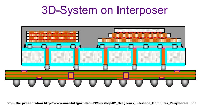
This diagram appears to show an entire system using a 3D stack of DRAM + a stack of other stuff:

b3da030.png


rather than a single GDDR6 DRAM.

Jawed
 
If you put the DRAM stack under the GPU the whole cooling problem disappears.
http://v3.espacenet.com/publication...=A1&FT=D&date=20090205&DB=EPODOC&locale=en_GB

Various stacked semiconductor devices and methods of making the same are provided. In one aspect, a method of manufacturing is provided that includes providing a first semiconductor die that has a first bulk semiconductor side and a first opposite side. A second semiconductor die is provided that has a second bulk semiconductor side and a second opposite side. The second opposite side of the second semiconductor die is coupled to the first opposite side of the first semiconductor die. Electrical connections are formed between the first semiconductor die and the second semiconductor die.
I have to admit, I'd forgotten about this.

Jawed
 
The roadmap goes GDDR5+ then GDDR6. GDDR6 will look a lot like mainstream DDR4, or maybe the other way around, but big changes in any case. You will see the first GDDR5+ parts on the market in Q1 or so (note: this means GDDR5+ chips, not necessarily anything mainstream that uses them).

-Charlie
 
The only really big change they can do with DDR4 is going with differential signalling and daisy chaining (FB-DIMM redux). The impact on GDDR won't be as big though, it doesn't need daisy chaining and because the signal integrity is already pretty decent the extra traces/pins necessary for differential signalling eat into the gains much more heavily than for DDR (ie. Qimonda estimated 2 times gain in bandwidth per pin for signalling on the motherboard, and an actual reduction in bandwidth per signal pin for a GPU PCB).
 
Has anyone tried cooling these stacks with carbon nanotubes? They have tremendous surface area and are good thermal conductors. I wonder if they could be grown like grass on the surface of each layer (kind of like these guys have done in their ultra-capacitor project http://www.technologyreview.com/article/23197/ but not as dense) and then cooled with laminar air flowing between the stacked layers.
 
If you put a DRAM die below the gpu die, wouldn't it need a custom DRAM die? And wouldn't that imply that both IHV's will have to make gpu dies (in a way) socket compatible? Not to mention that this solution is probably unworkable for LIano/ontario like chips.

In the short term, making a gpu+gddr MCM would be a better idea.
 
If you put a DRAM die below the gpu die, wouldn't it need a custom DRAM die?
So? GDDR5 was essentially custom DRAM made for ATI.
And wouldn't that imply that both IHV's will have to make gpu dies (in a way) socket compatible?
No, only the layout of the DRAM I/O and the locations of TSVs through the DRAM would "have" to be identical (you probably still want to have power/ground pins at least in the area over the DRAM, so those have to be passed through the DRAM with TSVs). In theory you could reroute even the DRAM I/O however you wanted with silicon interposers, but it doesn't seem very economical.
 
NV went on to use gddr5 which makes it custom only for a very short period.

And what about making gpu's with different sized memory buses and different amount of power pins? Can a single dram die be made to serve these two purposes without excessive cost penalty?

I am assuming that the cost of dram die will go up in proportion to the number of TSVs required.
 
Back
Top