first generation PS2 EE: 13.5 or 10.5 Mtr??

Think about the EE+GS@90nm, it does not use only 90 nm parts (65 bn gate length) on all the chip, that is where the SI vs Chipworks debate started from.

Think why those chip revisions for the EE, #2 and the #3, are in the middle of the manufacturing nodes generations.

This would explain the difference in area (if you also take into account layout and routing optimizations).
 
Jaws said:
Archie4oz said:
...
ASC7PL (.18µm) became available Q4 FY99...

:?

and "aviable" is different of "use in all chip immediatly and for a mass production"

Quaz51 said:
the 180nm process was used maybe at first for product the GS of the first PS2, in fact the GS2 188mm² for the launch of the PS2 was probably in 180nm (compared at GS1 279mm² in 250nm, the difference is big) but the EE2 at launch of the PS2 was again in 250nm
this for me the best and more logic explication
 
Panajev2001a said:
Think about the EE+GS@90nm, it does not use only 90 nm parts (65 bn gate length) on all the chip, that is where the SI vs Chipworks debate started from.

Think why those chip revisions for the EE, #2 and the #3, are in the middle of the manufacturing nodes generations.

This would explain the difference in area (if you also take into account layout and routing optimizations).

for the GS probably because the process of eDRAM and Logic are sometime different but for the EE i don't think
 
and i think that you assign overly importance at this graph (the graph with all chip's version) that is probably very approximate when a lot official doc say 224mm²=250nm process, it's not reasonable :)
 
i think the GS2 188mm² for the PS2 launch is maybe a 180nm logic + 250nm eDRAM
and the GS3 would be the first full 180nm, this is my impression when i see the micrograph's appearence in the roadmap graph
 
Panajev2001a said:
Think about the EE+GS@90nm, it does not use only 90 nm parts (65 bn gate length) on all the chip, that is where the SI vs Chipworks debate started from.

Think why those chip revisions for the EE, #2 and the #3, are in the middle of the manufacturing nodes generations.

This would explain the difference in area (if you also take into account layout and routing optimizations).


thanks Pana, for saying ''revisions for the EE, #2 and #3. instead of the very confusing (at first) EE2 and EE3 :)
 
Quaz51 said:
i think the GS2 188mm2 for the PS2 launch is maybe a 180nm logic + 250nm eDRAM
and the GS3 would be the first full 180nm, this is my impression when i see the micrograph's appearence in the roadmap graph

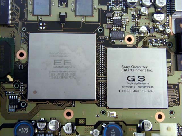
That sounds very plausible...here's the launch mobo and chipsets...

ps220040.jpg


So does the 188mm2 launch GS have a difference in transistor count from the 279mm2 GS?
 
Back
Top