ELSA hints GT206 and GT212

Nope. The TMUs are right next to the ALUs and should be much larger. The layout of the TMUs of this chip must be irregular.

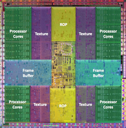
GT200:
gt200marked.jpg


red = Vec8
green = octo TMU.

3xVec8 + octo TMU = TPC.

What you have marked as ROPs+TMUs ist most likely the GDDR5 interface.
 
Last edited by a moderator:
GPU-Z/VR-Zone's reporting the wrong shader count, 24 instead of 16, on GT218.
Hmm, I've been told that NVidia's specifications page is wrong and it's 24.

So that would appear to indicate the entire line-up is based upon 3 multiprocessors with a pair of quad TMUs per cluster.

So TMUs appear to be:
  • GT218 - 8
  • GT214 - 16
  • GT215 - 32
Jawed
 
Nope. The TMUs are right next to the ALUs and should be much larger. The layout of the TMUs of this chip must be irregular.

GT200:
gt200marked.jpg


red = Vec8
green = octo TMU.

3xVec8 + octo TMU = TPC.

What you have marked as ROPs+TMUs ist most likely the GDDR5 interface.

I know it's this way with GT200 and older chips. GT21x are a new breed and 'til now, I fail to identify the TMU area(s) on those GPUs.
 
3xVec8 + octo TMU = TPC.
What you've marked doesn't add up to an entire cluster. Could be general control or it could be TMU. Dunno.

Also, what's interesting is that in the GT215 die shot the clusters appear to contain much less logic than GT200 (the ratio of area for "ALUs" to "TMUs" is wildly different comparing the two) - implying that the layout of GT215 doesn't have clusters as single contiguous units.

Either that or there's much less TMUs. Or that scaling to 40nm has been wildly non-linear depending upon unit :???:

The scaling of the ALUs, for what it's worth, appears to be ~2x, from 65nm GT200 to 40nm GT215. One "ALU" in GT200 is 0.654mm² and the same unit in GT215 is 0.323mm².

Jawed
 
There are four similar structured rectangle blocks, situated between the pairs of TPCs distinguishable in the die shot -- those could be texturing hardware, being just the samplers, mapping units or even both (too small for eight TMU quads, anyway... duh!). :???:
 
What you've marked doesn't add up to an entire cluster. Could be general control or it could be TMU. Dunno.
Its oddly marked, that's for sure, but there's obviously 10x(3x+1) instances.

For the die shot linked to, I don't believe the areas marked 'SIMD' should cover the area that they do. Each SIMD block does seem to represent 3x of something, but the piece attached to it (which I'm saying shouldn't be part of it) isn't a duplicate on each of the different blocks. It might be a routing issue that's making them look different (and they're only instanced on lower metal layers), but I kinda doubt that.

I don't think that what that person has labeled as the same thing on the lower and left hand edges are actually the same thing.

What I see is
4x(3x)--what's mark SIMD
8x --what's marked octo-dunnos
8x --what's marked QTU on the left
4x --what's marked QROP of the left
8x --what's marked QTU on the bottom
4x --what's marked QROP on the bottom

I'd gather that there are 4 functional units, each composed of:
3x something (SIMD)
2x something (QROP of the left)
2x something (QROP of the bottom)
2x something (OCTO on teh top)
1x something (QTU on the left)
1x something (QTU on the bottom)
 
Its oddly marked, that's for sure, but there's obviously 10x(3x+1) instances.

For the die shot linked to, I don't believe the areas marked 'SIMD' should cover the area that they do.
Agreed.

Each SIMD block does seem to represent 3x of something, but the piece attached to it (which I'm saying shouldn't be part of it) isn't a duplicate on each of the different blocks. It might be a routing issue that's making them look different (and they're only instanced on lower metal layers), but I kinda doubt that.

I don't think that what that person has labeled as the same thing on the lower and left hand edges are actually the same thing.

What I see is
4x(3x)--what's mark SIMD
8x --what's marked octo-dunnos
Appears to be PCI Express
8x --what's marked QTU on the left
4x --what's marked QROP of the left
8x --what's marked QTU on the bottom
4x --what's marked QROP on the bottom
IO connections for GDDR, with what's labelled QROP actually prolly corresponding with command bus with the remainder being data bus.

Jawed
 
How sure are you about that?

Those seem awfully busy and large to be pads and drivers for 4 pins for each square.
 
I think fellix's ideas are on the right track, though the "stacked" stuff is quite a puzzler.

Carsten if you compare with the annotated GT200 here (even if there are some who doubt its accuracy):

http://www.techreport.com/articles.x/14934/2

you should see that TMUs and ROPs take up acres of space.

Jawed

That shot doesn't distinguish at all between SIMD-Control- and TU-logic - it's all "Texture", whereas the GT21x-shot at least shows some additional logic besides the actual ALUs in the SIMD-parts of the die - but just not enough to make me believe, that TUs are still incorporated.

I'm not saying, fellix is wrong and I am here, but I've yet to see convincing evidence for either position.

And take into account, that for DX10.1 Nvidia would have to overhaul their TMUs either way - and maybe they tried to get away with less space, maybe combining some of the stuff for accessing memory, which is replicated in both TMUs and ROPs.

I could imagine, you can get away with less space when routing a dual-lane (1 for ROP-use, 1 for TU-use) to memory compared to having to to the individual routing from two far away parts of the die (I guess that's the principle of highways or autobahns also).
 
There are four similar structured rectangle blocks, situated between the pairs of TPCs distinguishable in the die shot -- those could be texturing hardware, being just the samplers, mapping units or even both (too small for eight TMU quads, anyway... duh!). :???:
Just to make my statement more figurative (the red outline):

gt215.png
 
That shot doesn't distinguish at all between SIMD-Control- and TU-logic - it's all "Texture", whereas the GT21x-shot at least shows some additional logic besides the actual ALUs in the SIMD-parts of the die - but just not enough to make me believe, that TUs are still incorporated.
Try this, too:

http://pc.watch.impress.co.jp/docs/2008/0617/kaigai_16l.gif

Even though it, too, doesn't make the distinctions you require.

I agree there should be some control stuff per cluster and I've no idea of the extent of the SIMD-specific stuff (i.e. 3x MAD-8, MI-2 and DP-1).

And take into account, that for DX10.1 Nvidia would have to overhaul their TMUs either way - and maybe they tried to get away with less space, maybe combining some of the stuff for accessing memory, which is replicated in both TMUs and ROPs.
Yes, they definitely have to do extra things (e.g. gather). We still don't even know how many TMUs there are. For all we know there's only 16 of them :p

I could imagine, you can get away with less space when routing a dual-lane (1 for ROP-use, 1 for TU-use) to memory compared to having to to the individual routing from two far away parts of the die (I guess that's the principle of highways or autobahns also).
Yes, to a degree "repeater islands" across the die imply that routing will agglomerate. The routes themselves don't take space since they are in metal layers under the logic layer.

Jawed
 
What you've marked doesn't add up to an entire cluster. Could be general control or it could be TMU. Dunno.
What's missing? NVIDIA marks it the same.

Just to make my statement more figurative (the red outline):

gt215.png
Hrm that could explain it. But then that NVIDIA picture is wrong:

gt200.jpg


There should be more "random" logic that is not texture that belongs to the ALUs.
 
Just to make my statement more figurative (the red outline):

gt215.png
The red squares don't look to be instances. The contents look similar, but they don't look like instances.

And the blue squares seem to be too big. (the areas closer to the center line do not match across instances)
 
I think we've already concluded here, that irregularities between similar block instances are due to employing a full automatic design & tuning for the selected logic circuits.
 
What you're pointing to doesn't look like a sea of gates, either (i.e. the product of automatic place and route).

I mean, I guess it just doesn't make sense to me to 'halfway instance' something in a way that looks close to the same, but not quite.

Usually instancing is either plopping hard macros down, or just letting the auto place and route do its thing and ending up with a sea of gates.

Of course, I only tangentially work in the back end of chip design, so I just might not be familiar with the technique.
 
Back
Top