ELSA hints GT206 and GT212

Nice die shot, too bad the quality is too low to clearly see what is copy-pasted and what is not, and which blocks are the same ones but synthesized multiple times
Maybe this one is better?

10pzgaq.jpg


I wonder if it's only two GPUs really with 230/240 and 250/260 using the same GPU but with half of TPCs in 230/240 case...
That would mean that 214/215 is still somewhere out there...
 
Their high-end has moved to 55 nm quite recently (January this year, I believe?), and shrinking to 40 nm so soon would probably make the 55 nm shrink a poor investment.
Bear in mind that G94, G96 and GT200 all had 65nm and then, within a few months, 55nm versions. Only G92 had a long interval. The interval seemed longer because NVidia had so much 65nm inventory. So while short intervals imply wasted money, the process nodes have mucked things up on a fairly substantial scale this last 18 months.

So the 9800/GTS250-range would be the most logical target for 40 nm... But... that product line is getting VERY long in the tooth. Do they really want to shrink that architecture yet again?
I have been expecting GT200 to be shrunk, with a performance increment (i.e. more ALUs and prolly more TMUs).

The biggest of these newest GPUs are essentially G92 shrunk to 40nm (admittedly with a bit of a shortfall in ALUs & TMUs - but that didn't hurt G94 much in comparison with G92) with added features (D3D10.1) and tweaks (some GT200 texturing efficiency and register file sizing?). So there's no need to do any more shrinking for GPUs below GT200.

These prolly should have been here last November, but who knows, eh?

Will they have a 40 nm GT200 as mainstream parts, with a GT300 high-end?
Seems pretty likely to me, for what it's worth. There'll be a huge performance gap between GT300 and GT215 - assuming that the largest of these NVidia GPUs is indeed GT215.

Jawed
 
I wonder if it's only two GPUs really with 230/240 and 250/260 using the same GPU but with half of TPCs in 230/240 case...
That would mean that 214/215 is still somewhere out there...
It wouldn't be surprising, since NVidia needs some kind of redundancy.

Unless what's actually just launched is a single GPU :oops: Turning off half the ALUs/TMUs for the crappy GT240M/GT230M. And additionally turning off half the memory and ROPs for the shitfactor G210M.

Holy fuck.

Jawed
 
Bear in mind that G94, G96 and GT200 all had 65nm and then, within a few months, 55nm versions. Only G92 had a long interval. The interval seemed longer because NVidia had so much 65nm inventory.

True, but the G94 and G96 are also higher volume parts, so you can get your return on investment more quickly.

The biggest of these newest GPUs are essentially G92 shrunk to 40nm (admittedly with a bit of a shortfall in ALUs & TMUs - but that didn't hurt G94 much in comparison with G92) with added features (D3D10.1) and tweaks (some GT200 texturing efficiency and register file sizing?). So there's no need to do any more shrinking for GPUs below GT200.

Well, that is if you don't make any distinction between mobile and desktop chips.
Currently these 40 nm chips are only for mobile parts. Which means the desktop line still needs a shrink (even though nVidia has already done the work for it with the mobile line). The production of desktop parts is still limited to 55 nm. Hence my question... when nVidia puts 40 nm desktop parts into production, will they be derivatives of this mobile line, or will they go for something else on the desktop?

Seems pretty likely to me, for what it's worth. There'll be a huge performance gap between GT300 and GT215 - assuming that the largest of these NVidia GPUs is indeed GT215.

That is what you'd expect, given the past strategy of nVidia. The 8800 series launched as high-end first. Everything else was just last gen's DX9 hardware.
By the time the 8600 arrived, they had already revamped the core logic a bit.
Just wondering if that strategy isn't a bit dated now. Then again, Intel still does it with their CPUs aswell.
 
Seems pretty likely to me, for what it's worth. There'll be a huge performance gap between GT300 and GT215 - assuming that the largest of these NVidia GPUs is indeed GT215.

Jawed
Even if we assume that GT215 isn't that 96 SPs / 32 TUs chip but some kind of a bigger G92b replacement (192 SPs, 64 TUs, 192-bit GDDR5?) the gap between it and 512 SP 512-bit GDDR5 G300 is still quite large.
GT212 cancellation may mean something here. I hope that some kind of G30x middle class GPU (~256 SPs, 256-bit GDDR5?) which should fill this gap left by GT212 cancellation isn't that far off...
 
Looking at these pictures:

G210M:
http://www.pcgameshardware.com/&menu=browser&mode=article&image_id=1144031&article_id=687342&page=1

GT230M
http://www.pcgameshardware.com/&men...104&image_id=1144035&article_id=687342&page=1

GT240M
http://www.pcgameshardware.com/&men...104&image_id=1144039&article_id=687342&page=1

there's at least 2 GPUs in this range (though "GT240M" versus "GT230M" looks like a photochop). So there doesn't seem to be an MC and/or ROP redundancy option amongst these SKUs.

Considering that the 128-bit memory bus should occupy around 18mm of perimeter (RV770's 256-bit bus occupies 36mm of perimeter), is it reasonable to guess that the biggest of these is about 11.3x12mm, 137mm²?

If this biggest chip is: 96 MADs+24MULs, 32 TMUs, 16 ROPs, 128-bit at 137mm², it makes for an interesting comparison with RV740's 640 MADs, 32TUs, 16 RBEs and 128-bit bus, doesn't it?

Put another way, this chip can do one MAD for 96 pixels in parallel while RV740 can do 5 MADs for 128 pixels in parallel. Even adjusting for clocks and counting the MUL, this NVidia GPU's compute density seems pitiful.

Does this new GPU have double-precision?

Jawed
 
Well, that is if you don't make any distinction between mobile and desktop chips.
Why would NVidia make a distinction?

Are the prior mobile GPUs distinct from the desktop GPUs? (I don't honestly know, for what it's worth).

Jawed
 
Why would NVidia make a distinction?

Are the prior mobile GPUs distinct from the desktop GPUs? (I don't honestly know, for what it's worth).

In a way they are, yes. At the very least they are clocked lower than their desktop counterparts and/or binned differently. After all, mobile GPUs need to work under different heat and power requirements. So you'd need to have a slightly different validation process at least.
Mobile parts may also be built on a slightly different manufacturing process, focusing less on maximum performance, but more on minimum leakage and/or size.
In some cases, mobile GPUs also have the video-memory on the GPU package. So they are physically different.
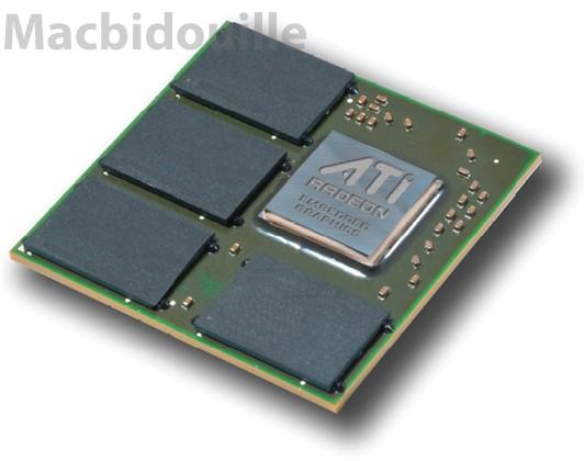
For example, this ATi Mobile Radeon 4690:
e4690.jpg


The question 'why' isn't that important, since clearly nVidia DOES make the distinction. They specifically announced mobile parts, no sign of any desktop parts at 40 nm and with DX10.1 yet.
 
Last edited by a moderator:
Put another way, this chip can do one MAD for 96 pixels in parallel while RV740 can do 5 MADs for 128 pixels in parallel. Even adjusting for clocks and counting the MUL, this NVidia GPU's compute density seems pitiful.

Wasn't that difference in "peak" compute density already baked into the architectures since R600/G80? Given the different approaches what compute density would you consider to not be pitiful?
 
In a way they are, yes. At the very least they are clocked lower than their desktop counterparts and/or binned differently.
If these chips are expensive for the foreseeable future (because 40nm yields will ramp very slowly) and that existing 55nm chips are cheaper in their desktop incarnations, then you might be on to something. But in terms of the chips, technologically, I don't see anything that restricts them from being used as desktop parts.

Jawed
 
Wasn't that difference in "peak" compute density already baked into the architectures since R600/G80? Given the different approaches what compute density would you consider to not be pitiful?
All of this is conditional on the die size of this new chip. Also remember that feature differences (D3D10.1) made a comparison against RV7xx problematic until now.

So, when someone measures it, and when the full specification is actually revealed, we'll have more to go on.

But, for what it's worth, this is looking more pitiful than GT200 versus RV770 implies - not surprising with the added features, but has NVidia also not benefitted from 40nm as much as AMD?

Since this isn't a desktop launch there's not much marketing muscle behind this, so we'll just have to wait it seems.

Jawed
 
If these chips are expensive for the foreseeable future (because 40nm yields will ramp very slowly) and that existing 55nm chips are cheaper in their desktop incarnations, then you might be on to something. But in terms of the chips, technologically, I don't see anything that restricts them from being used as desktop parts.

Well no, you COULD use mobile parts for discrete videocards... just like it is possible to use mobile CPUs in a desktop.
It's just that this rarely happens. Mobile parts are generally more expensive, and have lower performance than their desktop counterparts (eg a GTX280M is nowhere near as fast as a discrete GTX280).

And although nVidia could easily create desktop variations of the current line of mobile products, it is a specific action they have to take, because it requires a slightly different manufacturing and validation process. Until then, their partners simply cannot order any 40 nm desktop parts, and as such there won't be any 40 nm-based videocards on the market.
 
Well no, you COULD use mobile parts for discrete videocards...
Hopefully someone will come up with evidence one way or the other.

Clearly ATI is using the same die for both mobile and desktop in the case of RV740. I just don't know what NVidia has done historically.

Jawed
 
Clearly ATI is using the same die for both mobile and desktop in the case of RV740. I just don't know what NVidia has done historically.

Same die yes, but they do run at different clockspeeds, and probably also at different voltages, so they have different validation processes at the least.
I'm not sure if they even physically come off the same production line.
 
Maybe some do and some don't? Back in the X1000 era, ATI launched a few chips which used strained silicon manufacturing (RV530-derived Rad. Mobility X1700), and those were just for the mobile market.
 
What I am missing a bit are the TMUs, which where directly coupled to the SIMDs previously.
 
Looking at the 96sp die, the SIMD arrays are mostly a carbon copy of the GT200's ones, shrunken to the new process, of course, but the texture units are obviously no more aligned to the clusters [sort of]:

gt200mobile.png
 
If you rotate the SIMD-blocks to the same alignment, you'll see, that they're not the same size, nor identical otherwise wrt control logic (the "non-yellow-part").
 
tpc.png


Left: 40nm TPC
Right: 65nm TPC (w/ TMU)

Note: Images are not scaled to the corresponding process -- just for a viewing convenience!
 
Last edited by a moderator:
Back
Top