Install the app
How to install the app on iOS
Follow along with the video below to see how to install our site as a web app on your home screen.
Note: This feature may not be available in some browsers.
You are using an out of date browser. It may not display this or other websites correctly.
You should upgrade or use an alternative browser.
You should upgrade or use an alternative browser.
ELSA hints GT206 and GT212
- Thread starter AnarchX
- Start date

Could be a more loose alignment of the various blocks -- look at a hi-res die shot of GT200 and you'll notice how some of the TPCs are definitely looking a tad bigger, while in fact the building components are just a bit "shaken" off their places. ")
The control logic blocks are identical function-wise, despite looking a bit different each other -- that is due to the extensive use of automated process for optimal placement instead of hand-tuned circuits, used only for the critical parts.nor identical otherwise wrt control logic (the "non-yellow-part").
Last edited by a moderator:
I'm still skeptical. Those are too far apart for my taste to be attributed to automated circuitry placement variations. Plus, the SIMDs also look different than GT200s ones - at least for a 1:1 copy.
Did anyone come up with a decent theory on the blue marked regions btw?

Did anyone come up with a decent theory on the blue marked regions btw?

Would it be fair to assume that the substrate on these are the same size, or at least for the 260 and RV740, which are both 128bit, gddr5 etc?
And in that way determine the die size (sure, all 3 are 3d renders, but I guess the scale is correct).
In that case I get basicly the same size for both.
And do we have any hard info on the number of ROPS in GTS260M?
Last edited by a moderator:
Just for fun...
Looking at the die and package shots nvidia provided for G210m(under additional images) here, can see die is almost exactly 1/3 the package size.
Back in January vr-zone had a gt218 P692 (GDDR3?) board which via PCI-E specs gave the package size as 22.6x22.6mm. Which implies the die size is 22.6mm / 3 = 7.67mm or 58.8mm2 die area for the G210m.
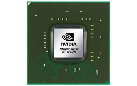
Similarly fudzilla reckon the package size for the GT216 was 29mm. Looking at the GT240m that is also almost exactly 33% width and length of package size implying 29 x 0.33 = 9.66mm for die sides => die size of GT240m is 93mm2
Of course could have changed the packaging in the intervening 6 months or use different packaging for mobile and desktop parts...
Looking at the die and package shots nvidia provided for G210m(under additional images) here, can see die is almost exactly 1/3 the package size.
Back in January vr-zone had a gt218 P692 (GDDR3?) board which via PCI-E specs gave the package size as 22.6x22.6mm. Which implies the die size is 22.6mm / 3 = 7.67mm or 58.8mm2 die area for the G210m.
Similarly fudzilla reckon the package size for the GT216 was 29mm. Looking at the GT240m that is also almost exactly 33% width and length of package size implying 29 x 0.33 = 9.66mm for die sides => die size of GT240m is 93mm2
Of course could have changed the packaging in the intervening 6 months or use different packaging for mobile and desktop parts...
Last edited by a moderator:
Now for heroic leaps....
Looking at the G210m and GT240m on the nvidia site under additional views for each chip the die shot and a shot of the pin layout.
Ok from previous post i get that G210m is 57mm and GT240m is 93mm ie GT240m is 1.65 times.
Flipping the package over and looking at the pins, if can make the really big assumption that the minimum distance between the pins will be constant between the 2 packages...i get that GT240m is 1.64x the size. This is close enough to the above measure to take this foolish leap...
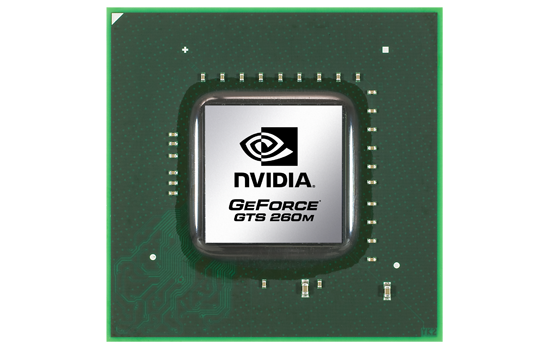
Looking at GTS260m from measuring the pins and assuming constant separation gives it as 2.12x the size of the G210m.
ie by constant pin separation GTS260m is 121.5mm2
Obligatory caveat about the laughable reliability of this calculation: by constant pin separation the GTX280m is 2.87x the G210m size ie 167mm2 or a third less than it actually is in real life
Looking at the G210m and GT240m on the nvidia site under additional views for each chip the die shot and a shot of the pin layout.
Ok from previous post i get that G210m is 57mm and GT240m is 93mm ie GT240m is 1.65 times.
Flipping the package over and looking at the pins, if can make the really big assumption that the minimum distance between the pins will be constant between the 2 packages...i get that GT240m is 1.64x the size. This is close enough to the above measure to take this foolish leap...
Looking at GTS260m from measuring the pins and assuming constant separation gives it as 2.12x the size of the G210m.
ie by constant pin separation GTS260m is 121.5mm2
Obligatory caveat about the laughable reliability of this calculation: by constant pin separation the GTX280m is 2.87x the G210m size ie 167mm2 or a third less than it actually is in real life
Last edited by a moderator:
Jawed
Legend
Might also be worth correlating with the GPU being "replaced", e.g. G94 being replaced by GT215 (GTS260M), since it seems likely that the package sizes are the same.Would it be fair to assume that the substrate on these are the same size, or at least for the 260 and RV740, which are both 128bit, gddr5 etc?
I'm dubious that RV740's substrate matches though (except coincidentally). Unless a common third-party cooler design influences things?
Nope, NVidia's being shy about ROPs and TMUs. ROPs scale with bandwidth and theoretically the smallest of these chips, GT218, has a single cluster of 16 ALU lanes, so prolly has 8 TMUs.And do we have any hard info on the number of ROPS in GTS260M?
The remaining question is whether these have had an overhaul as part of D3D10.1 changes or implementation of GDDR5
Jawed
Jawed
Legend
Ooh, that's nice.Just for fun...
Looking at the die and package shots nvidia provided for G210m(under additional images) here, can see die is almost exactly 1/3 the package size.
Back in January vr-zone had a gt218 P692 (GDDR3?) board which via PCI-E specs gave the package size as 22.6x22.6mm. Which implies the die size is 22.6mm / 3 = 7.67mm or 58.8mm2 die area for the G210m.
Similarly fudzilla reckon the package size for the GT216 was 29mm. Looking at the GT240m that is also almost exactly 33% width and length of package size implying 29 x 0.33 = 9.66mm for die sides => die size of GT240m is 93mm2
Both those sizes would seem to be targetting the minimum for 64-bit and 128-bit buses. Earlier I was querying the ability to design a GPU for minimum area for a given bus size on a process, when the process is very new (i.e. hard to be precise).
Now I'm wondering if the long gestation of a node (18 months?) from the time the libraries are available to the time production starts, means that the designer can be fairly precise?
Jawed
Jawed
Legend
Aha, that's pretty cool, though this caveat does screw things up.Obligatory caveat about the laughable reliability of this calculation: by constant pin separation the GTX280m is 2.87x the G210m size ie 167mm2 or a third less than it actually is in real life
For what it's worth, I get a different size for GT216, using the "additional views" pix from NVidia. Assuming the package is 29mm on each side, the chip is indicated to be 10.1mm per side, 102mm².
It seems to me that GT215 has the same package size as the balls are exactly the same. This leads to 11.9mm per side, 141.6mm².
If we assume 0.5mm of die encapsulation, then these come out as 92mm² and 130mm².
Jawed

Redoing the calc i get the same as above. Also 54.8mm2 for G210m. Originally i did it only using shot of the 2 chips one face up and one face down both of which were at different angles, tried hard to account for the perspective guess i slipped up somewhere though.For what it's worth, I get a different size for GT216, using the "additional views" pix from NVidia. Assuming the package is 29mm on each side, the chip is indicated to be 10.1mm per side, 102mm²
Afterwards noticed that there were also higher resolution straight up shots present...
It seems to me that GT215 has the same package size as the balls are exactly the same. This leads to 11.9mm per side, 141.6mm².
If we assume 0.5mm of die encapsulation, then these come out as 92mm² and 130mm².
Yes package does look very similar between both chips. If it is the same size then for the GTS260m i get just less than 140mm2
Not sure if i was imagining it, but thought i could see black bits sticking out from behind the silver covering they photoshopped on top on the GT240m and GTS260m images but not G210m.
Jawed
Legend
I think fellix's ideas are on the right track, though the "stacked" stuff is quite a puzzler.
Carsten if you compare with the annotated GT200 here (even if there are some who doubt its accuracy):
http://www.techreport.com/articles.x/14934/2
you should see that TMUs and ROPs take up acres of space.
Jawed
Carsten if you compare with the annotated GT200 here (even if there are some who doubt its accuracy):
http://www.techreport.com/articles.x/14934/2
you should see that TMUs and ROPs take up acres of space.
Jawed
It looks like the PCIe Phy interface is damn hard to scale than anything else.I think fellix's ideas are on the right track, though the "stacked" stuff is quite a puzzler.
By looking at the overall die, it definitely doesn't seem to be much pad limited -- the GDDR paddings are conveniently stretched all the way, without cornering or stacking, for that matter. You can clearly see the separation of command/address and data pads.
Apart from this maybe not being very accurate: In the GT200-Shots, there's two vertical units "above" each set of processing cores - AFAIK that was scheduling/control and the two quad-TMUs attached to each SIMD. Those are missing in the 40nm shots altogether and the control-part is attributed to "texture" in the picture from techreport.Carsten if you compare with the annotated GT200 here (even if there are some who doubt its accuracy):
http://www.techreport.com/articles.x/14934/2
Which you were one of the greatest critics of, IIRC.you should see that TMUs and ROPs take up acres of space.
I should have said I think PCI Express is that long thin section down the left hand side - compared with other die shots, PCI Express is thinner than DDR.
That stacked stuff might be GDDR5-specific. I dunno.
Excerpt from the GT200 die-shot:

The vertical row on the left side is the PCIe phy link -- the pattern looks very similar to the "stacked" one in the 40nm 96sp die.
Just a copy from the "nvidia strain" topic:
http://vr-zone.com/articles/nvidia-partners-get-ready-40nm-g210--gt-220-cards/7272.html?doc=7272
vr-zone reports mass production of 40nm won't start 'till August with mass availability for both laptop and desktop parts not expected till October, i.e. Win7 time.
http://vr-zone.com/articles/nvidia-partners-get-ready-40nm-g210--gt-220-cards/7272.html?doc=7272
vr-zone reports mass production of 40nm won't start 'till August with mass availability for both laptop and desktop parts not expected till October, i.e. Win7 time.
Similar threads
- Replies
- 70
- Views
- 22K
- Replies
- 52
- Views
- 25K
- Replies
- 32
- Views
- 10K
- Replies
- 4
- Views
- 14K