
Hmmm, cannot find any of the GTS chips anywhere, not sure what is going on, also the numbers overlap G92 - GTX260M and GT214/215 - GTS260M which i dont think they have done before. Also was sure this chip was physically bigger, enough at least to support a 192bit interface....apart from the obvious GDDR5 support wondering why they have released 2 chips with 128bit interfaces.
You are using an out of date browser. It may not display this or other websites correctly.
You should upgrade or use an alternative browser.
You should upgrade or use an alternative browser.
ELSA hints GT206 and GT212
- Thread starter AnarchX
- Start date
According to Tech Report, the new chips indeed support DX10.1, and are GT2xx based, not G9x
Jawed
Legend
http://www.nvidia.com/object/geforce_m_series.html
PhysX is not supported on GT240M, GT230M and G210M. D3D10 is listed, not 10.1.
Jawed
PhysX is not supported on GT240M, GT230M and G210M. D3D10 is listed, not 10.1.
Jawed
Jawed
Legend
Seems NVidia's specifications page for these GPUs is erroneous, as the Features page says this:
JawedHigh Performance GeForce DirectX 10.1 Graphics Processor
NVIDIA® GeForce ®GTS enthusiast class GPUs include a powerful DirectX 10.1, Shader Model 4.1 graphics processor, offering full compatibility with past and current game titles with all the texture detail, high dynamic range lighting and visual special effects the game developer intended the consumer to see. Water effects, soft shadows, facial details, explosions, surface textures and intricate geometry create cinematic virtual worlds filled with adrenalin pumping excitement. Of course all these special effects run at high resolution and playable frame rates for immersive heart-pounding action.
Why no texturing specs?
That would give it all away, no?

I suspect that even with the purported distancing from G9X, the parts are pretty still much based on the same clustering, and castrated for initial yields. DP SFUs? I don't think so.
Would the following scenario hold true?
G92c with 128-bit bus and GDDR5 support plus some tweaks to support DX10.1?
G94c, and G96c on 64-bit (brutal halving of SPs as of now, scary)
128 - > 96
64 -> 48
32 -> 16
I think it's 100% clear when Matt Wuebling says "Leverage the architecture of our Previous Desktop GPU's" in this Hexus interview.
http://tv.hexus.net//show/2009/06/COMPUTEX_2009_NVIDIA_launch_new_notebook_GPUs/
And then goes on to "based on a different architecture"
Does nVidia actually know what their GPU's are based on.
http://tv.hexus.net//show/2009/06/COMPUTEX_2009_NVIDIA_launch_new_notebook_GPUs/
And then goes on to "based on a different architecture"
Does nVidia actually know what their GPU's are based on.
I am a bit confused. So what chips are those new mobile cards using???
The 16 SP part more looks like a G92 derivative, while the other ones more like G200 derivative (not only because of the 16 SPs but also because it reaches a higher shader clock than any of the others, similar to what we see on desktop g92 vs g200).
Otherwise these chips look somewhat decent to me, particularly since they seem to have reasonable TDP. Now, the better-than-IGP G210M definitely looks a bit slow, the GT230M/GT240M however could compete quite well against some AMD parts (I doubt the GT240M can touch the HD4670 Mobility if both are using the top-end configuration, but a lot will depend on actual memory (clock) used - Nvidia now also (or did they before) support ddr3, but HD4650 Mobility should be in range I guess).
GTS250M/GTS260M also don't look too shabby, they might be slower than the top-end nvidia mobile chips but have way more reasonable power draw (though the GTS260M is quite bad compared to GTS250M here). Neither one will be able to touch HD4860 Mobility but HD 4830 Mobility should be in range I guess (particularly versions using GDDR5 - way less compute power than HD 4830 but way more memory bandwidth).
Not really hard to guess:I am a bit confused. So what chips are those new mobile cards using???
G 210 = GT218
GT 230/240 = GT216
GTS 250/260 = GT215
I don't think that you may make any assumptions about GPU features from SP numbers and shader domain frequencies.The 16 SP part more looks like a G92 derivative, while the other ones more like G200 derivative (not only because of the 16 SPs but also because it reaches a higher shader clock than any of the others, similar to what we see on desktop g92 vs g200).
NV's saying that they all support 10.1 plus 250/260 support GDDR5 which means new ROPs are a given. That makes them more than a derrivatives of anything, closer to GT200 evolution. (Probably why they're called GT21x.)
So... What's this?

Ideas anyone?
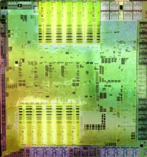
[edit]OK, this looks to be good old G92 again. Wonder what's it doing in GT21xM announcement...[/edit]
Last edited by a moderator:
Jawed
Legend
Maybe NVidia's saving the full 128 ALU lanes version for desktop? Or even mobile, when the yields improve (GTX270M, say).
Ideas anyone?
[edit]OK, this looks to be good old G92 again. Wonder what's it doing in GT21xM announcement...[/edit]
Jawed
Maybe the colon represents a dual GPU solution comprised of very tiny chips?Nice. GT215 is the first invisible GPU!
-FUDie
Sorry I forgot that direct links don't work from hardware.fr. You can get the picture there : http://www.hardware.fr/news/10283/40nm-gddr5-dx-10-1-nvidia.html
So, it's official now... nVidia has DX10.1 support. And 40 nm aswell
I wonder if the other rumours are true aswell... that there will be desktop-derivatives of these new DX10.1 chips soon.
I've especially doubted that because where would that leave the DX11 parts? But you could say it's wishful thinking. I mean, I suppose most of us will want to see DX11 parts from both nVidia and AMD... but there is a possibility that nVidia's chips are delayed, so there will be a 40 nm DX10-refresh first, and that refresh may include DX10.1 support, just as on the mobile side.
Jawed
Legend
It's fairly normal, with the introduction of a new GPU design, for the cheaper SKUs from the prior generation to hang around for a while until they're replaced by cheaper members of the new family. G80 was alone until G84 arrived 5 months later.
Apparently GT2xx family has only just been filled out with its smaller variants.
It seems unlikely that GT300 will be joined by cheaper members simultaneously. Unless the machinations at 40nm crunch everything up. Given that 3 GPUs have just launched simultaneously, maybe something similar could be repeated with GT300.
It'll be interesting to see if AMD's supposed lead means that there'll be several D3D11 ATI chips on the market by the time that GT300 launches, as part of AMD's strategy is faster family fill-out. RV770, RV730 and RV710 all arrived within 3 months of each other.
Jawed
It seems unlikely that GT300 will be joined by cheaper members simultaneously. Unless the machinations at 40nm crunch everything up. Given that 3 GPUs have just launched simultaneously, maybe something similar could be repeated with GT300.
Historically nVidia has always started on a new process with lower-end chips first, to 'test the waters'...
If these mobile 40 nm parts are the 'testing the waters'-phase, then GT300 is probably still a few months off (assuming it's 40 nm, and not 55 nm... but I think that's a safe assumption).
In that light I think there is room for some lower-end 40 nm desktop parts aswell.
But looking at the actual desktop product line from nVidia, I'm not sure where it would fit in... Their high-end has moved to 55 nm quite recently (January this year, I believe?), and shrinking to 40 nm so soon would probably make the 55 nm shrink a poor investment.
So the 9800/GTS250-range would be the most logical target for 40 nm... But... that product line is getting VERY long in the tooth. Do they really want to shrink that architecture yet again?
So the way I see it, putting 40 nm on the desktop at this point wouldn't be a very good investment. They'll probably want to wait a few months, then shrink GT200 to 40 nm, and replace the older G92-based product line with it.
But that all depends on how GT300 is going. Will they have a 40 nm GT200 as mainstream parts, with a GT300 high-end? Or will there be mainstream GT300 variations at launch? Or perhaps GT300 is more than just a few months off?
Similar threads
- Replies
- 70
- Views
- 19K
- Replies
- 52
- Views
- 23K
- Replies
- 32
- Views
- 8K
- Replies
- 4
- Views
- 13K