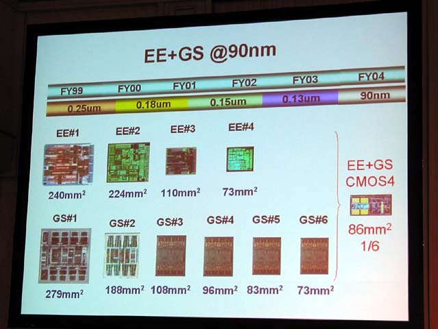
DM's 65 nm transistor density analysis based on Sony EE data

sony1_03.jpg


Sony EE gate density

0.250 um : 13 million / 224 mm2 = 0.058 million/mm2
0.180 um : 13 million / 110 mm2 = 0.118 million/mm2
0.150 um : 13 million / 73 mm2 = 0.178 million/mm2
0.090 um : 13 million / 42 mm2 = 0.310 million/mm2
0.065 um : ~ 0.594 million/mm2

Based on this Sony processor gate transistor density calculation of 0.594 million/mm2 at 65 nm, let's presume that Sony reaches for the max and shoot for a 280 mm2 chip, the largest Sony could swallow for consumer application.

280 mm2 * 0.594 million/mm2 = 166.32 million transistors

Meaning SCEI has a maximum budget of 166 million transistors for EE3 if it is to be built like previous EE, with lots of FPUs and little memory.

Now, does 166 million transistors sound enough to pack 4 PPC cores and 32 VUs??? Of course not. This is why I suspect that PSX3 CPU will have a single or dual CELL cores, not quad-core as many speculate. EE3 will never reach 1 teraflops even in the lab, mark my word on it.
 
Dead,

You're full of shit. plain and simple. ATI gets ~105M transistors out of much, MUCH less than 280sqmm at .15u! Does ANYONE, including yourself, doubt you're full of shit by now?

I can't believe alarm bells didn't go off like fireworks in your head once you came up with that REDICULOUS figure. Did you really think one couldn't even get 200M transistors at 280sqmm at .65????????

For example, Toshiba has the world's smallest DRAM cell for .65u SOI process where the the transistor itself is the bit capacitor also. Still thinking they can only fit 166M on such a huge chip? You're not just silly here, you're plain *insert word implying a few cards short of a full deck*.

This is just yet another example of why you need to get your posting privileges revoked, because all you do is stir up trouble.


*G*
 
That logic is faulty logic.

One of the reasons for Sony and Toshiba to work with IBM is to get some of their semiconductor technology. IBM is a leader like Intel in the field of chip manufacturing. Sony knows it needs world class chip fabrication to have at least a chance at stopping Microsoft from taking over the console market.

The people that run Sony, Toshiba, IBM, Microsoft, ATI, Micron, Intel, and so on aren't dumb. To often it seems people are posting very extreme views pro and con on issues. It is going to be a long hard fight for both Sony and Microsoft in 2005/6.
 
...

ATI gets ~105M transistors out of much, MUCH less than 280sqmm at .15u! Does ANYONE
GPUs typically have fewer logic gates and lots of SRAM gates, so their design density is much highter.

This is not the case with Sony's processors, which tend to be logic gate heavy and SRAM gate light. This is why their transistor density is low.

Take a look at Sony's Handheld engine, which has 1.35 million gates(Roughly 6 million transistors) but the silicon estate is equal to that of 8 MB eDRAM macro(70~80 million transistors)
 
...and why do we need 3 or 4 separate topics by DM? Why not just keep it all under one topic labeled, "Why DM thinks PS3 is utter crap"?

ANSWER: DM's posting behavior indicates an "agenda" to enforce a viewpoint, not to discuss on myraid console topics. Beats me why the powers that be haven't picked up on this (or they don't care, or they are fine with it altogether).

...and what sort of "PPC core" are we talking about, anyway? I was unaware that a specific generation had been disclosed (not saying it hasn't, I just haven't heard). Are we talking about a G3? 604? 601? What?
 
...

That logic is faulty logic.
Then you tell me why EE and GS has equal die size despite GS having more than three times as many transistors.

My logic is correct based on actual Sony production data.

PSX1 CPU -> PSX2 CPU -> PSX3 CPU

1 million->13 million ->166 million, the figures look about right, each generation having 13 times the transistor count of previous generation.

Once again, 4 PPC cores, 32 VUs, and 4 MB of cache will not fit into 166 million transistors.
 
The VUs take up only about a third of the EE, so at 65nm 1 VU1 should only take up ~4mm2. Fitting 32 VU1s shouldnt be a problem.

The register file is sizeable though, so assuming multithreading and larger caches that would grow quite a bit, with 4 PPC cores I wouldnt see it fitting either.
 
This is not the case with Sony's processors, which tend to be logic gate heavy and SRAM gate light. This is why their transistor density is low.

Those APUs seems to be more SRAM heavy, than logic gate heavy. 4 floating point units and 4 interger units. Not that much really.
 
...

Those APUs seems to be more SRAM heavy, than logic gate heavy. 4 floating point units and 4 interger units. Not that much really.
CELL VUs gain many additional features not found on EE VUs plus 128 KB cache, so the transistor count should go way up. Pipeline will have to be stretched to cope with higher clockspeed as well.
 
poor sony engineers thinking they could get 500M transistors on EE3 at .1micron all those yrs ago... What were they thinking? They must have been delirious... my sig it's so wrong...
 
This is why I suspect that PSX3 CPU will have a single or dual CELL cores, not quad-core as many speculate.

Than there would be no need for Sony to be taking a huge risk at 65 now would there. When 1 PE could be shoved right on 0.90 micron.

Oh and not many speculate this, only you and bbot both of which come from the depths of Teamxbox amoung other hangouts.
 
You can't just scale things like this DM. There isn't a fixed size for a transistor; that depends on the use. How else do you think we have Gigabit DRAM chips today?
 
But if you look at 90um, it seems that Sony is able to fit both EE and GS into 86mm2. GS has ~32 million non-EDRAM transistors. EE is another 13 (although I always thought it was 10.5 million).

(32 + 13) million / 86 mm2 = 0.64 million/mm2, which would be more then twice your 0.31 mm2 estimate. And that's without considering EDRAM transistor budget. (unless I am missing something).
 
BE/Cell/EE3 is ment to have:

-4 PPC-based (or MIPS-based) CPUs
-32 APUs
-either 36 or 68 MB of memory: (32~64 MB eDRAM plus 4 MB local memory, probably SRAM, split into 128K per APU)
 
Re: ...

DeadmeatGA said:
GPUs typically have fewer logic gates and lots of SRAM gates, so their design density is much highter.

No, this is wrong. GF3 is ~56M transistors, of which only a small minority is cache, according to what little inside info we have. I'm pretty sure the same holds true with later GPUs as well.

CPUs today are typically made up of at least 40% SRAM, and this looks to get "worse" as time passes. You made a bad mistake in your estimate, but of course you won't be man enough to fess up to it.

This is not the case with Sony's processors, which tend to be logic gate heavy and SRAM gate light. This is why their transistor density is low.

But you're no CMOS engineer! All you do is make stuff up! EE in its first incarnation was an enormous chip, to a large extent due to very few metal layers (four, I think), and the large amount of wide buses the chip uses. Lots of real-estate was lost due to this. Cell will be made with at least seven layers and perhaps even more!

Why can't you realize that you just DON'T UNDERSTAND these things, and that you can't simply scale things linearly like you're trying to do? I'm not a CMOS engineer either, that's why I don't try my hand at your rediculous, insane antics.

I'd insert a rolleyes here, but I'm starting to think that the constant, repetitive motion of all those eyes your posts are generating will wear out my computer system...

*G*
 
Back
Top