AMD: Pirate Islands (R* 3** series) Speculation/Rumor Thread

Going from the discussion at the (current) latest posts in the Volcanic Islands thread:

From eXtremeSpec: "AMD Pirate Islands Can be Announced The Summer."

The page links to a graphic containing claimed upcoming AMD GPUs and their specs:

R9 390X: Bermuda, 4224 CCs, 512-bit bus, October 2014.
R9 380X: Fiji, 3072 CCs, 384-bit bus, 2015.
R9 370X: Treasure Island, 1536 CCs, 256-bit bus, July 2014.

All on TSMC 20 nm. Note that most of these specs have question marks beside them.

If true then these chips should give the considerable performance jump that many have been waiting for. I think that 20 nm in July 2014 seems rather early though.
 
AIB partners said, reportedly, at CeBIT that they're expecting fall launch for Pirate Islands
 
AIB partners said, reportedly, at CeBIT that they're expecting fall launch for Pirate Islands
This would be perfect, i'd like to sell my 7950 and replace it with something more energy efficient but roughly the same performance.
With at least 4GB memory.
 
R9 390X: Bermuda, 4224 CCs, 512-bit bus, October 2014.
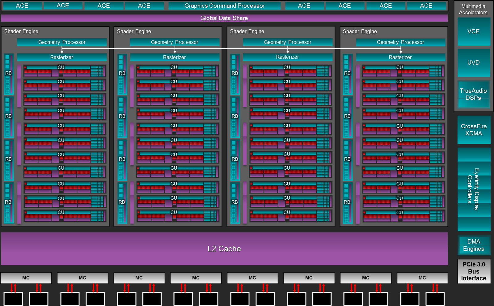
Weird... 66CUs?

6 * 12CUs, 1 disabled in each er... array? engine? what's the new terminology? pirate ship? booty?
pirate.gif


Something else?
 
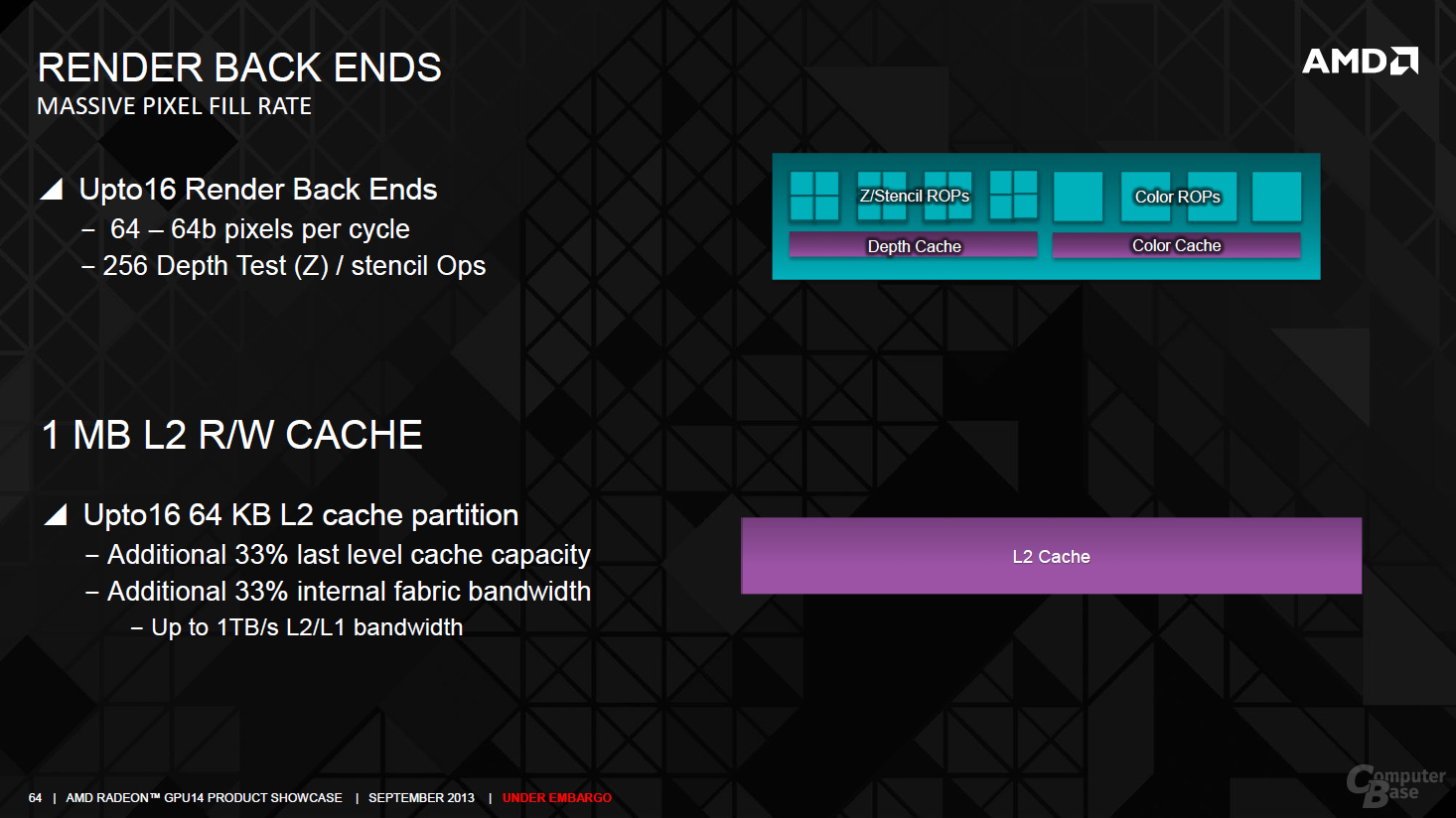
At any rate, I'd be more interested in changes to caches... (not sure what else to expect).


7.jpg


I really don't know, if it's true, but it looks like the L2-Cache scales now with the ROPs and not with MCs. Could just be a coincidence...
 
I really don't know, if it's true, but it looks like the L2-Cache scales now with the ROPs and not with MCs. Could just be a coincidence...

Can you clarify?
Tahiti has 768 KB of L2, 6 memory controllers, and 32 ROPs.
Hawaii has 1 MB of L2, 8 memory controllers, and 64 ROPs.
 
Can you clarify?
Tahiti has 768 KB of L2, 6 memory controllers, and 32 ROPs.
Hawaii has 1 MB of L2, 8 memory controllers, and 64 ROPs.

Thats a bit of a mystery, but I'll try:
For GCN 1.0, the L2-Cache is always coupled to the MCUs, which means the L2-Cache scales according to the number of the MCUs. The L2-Cache per MCU can be 128KB or 256KB.
Tahiti: 128KB per MCU -> 6 x 128KB = 768KB L2-Cache
Pitcairn: 128KB per MCU -> 4 x 128KB = 512KB L2-Cache
Cape Verde: 256KB per MCU -> 2 x 256KB = 512KB L2-Cache
Mars/Hainan: 128KB per MCU -> 2x128KB = 256KB L2-Cache
Bonaire: I dont know

For GCN1.1 aka Hawaii there seems to be a difference according to the presentation. First the ROPs are now part of the Shader Engines and not decoupled anymore, additional to that the L2-Cache looks like to be partitioned in a different way.
But thats just speculation...
 
I really don't know, if it's true, but it looks like the L2-Cache scales now with the ROPs and not with MCs. Could just be a coincidence...

Well, for APU integration I dont think you can really put your cache on DCTs, since they are shared with the CPU part. So it makes sense to decouple them from the memory controllers, I guess.
having the design already done, maybe they just reused it. Or maybe it offers additional benefits, especially in the optic of a unified address space? Who knows...
 
Thats a bit of a mystery, but I'll try:
For GCN 1.0, the L2-Cache is always coupled to the MCUs, which means the L2-Cache scales according to the number of the MCUs. The L2-Cache per MCU can be 128KB or 256KB.

Tahiti: 128KB per MCU -> 6 x 128KB = 768KB L2-Cache
Hawaii 128KB per MC -> 8 x 128KB = 1MB L2
What is the evidence of a change to the L2, aside from the L2 happening to be on the same marketing slide as ROPs?

Well, for APU integration I dont think you can really put your cache on DCTs, since they are shared with the CPU part. So it makes sense to decouple them from the memory controllers, I guess.
Current APUs actually maintain the GPU memory controller, and that then hops over to the physical memory controllers.
Yes, it is that hacky.

Unless the L2 is significantly changed and made capable of coherent snooping, it can't be decoupled from the memory controllers. The individual slices can only guarantee coherence and if they can only contain data from a linked memory channel.

Suddenly making an L2 slice capable of storing data from a non-exclusive set of memory devices will allow more than one slice to contain data from the same address.
If the same address cannot exist in more than one slice, why decouple it?
Yeah, the 'garlic' bus is essentially what connects the GPU MCT to the CPU DCTs.
But I was under impression that they did change the design to unify the L2 so it was not sliced any more.... ah well, maybe I was wrong.
 
Guys, take a look at what's going on there, page 3, comment 17: :LOL:

I'm theorizing a few things.

1. The R9-390x spec might actually be true. When Titan was first released, AMD was going to produce a graphic card with twice the amount of SP to the 7000 series card. This could never be done on 28, but it was possible for it to be on 20 nm. I believe the card was called Tenerife II. It was suppose to have twice the SP of a 7980 and 16 additional SP in series. Now that 20nm graphic are starting to make their appearance, it's possible that Bermuda XTX is actually Tenerife II v1.5.

Look at it from this point of view:
AMD 7980: 2048 SP at 975 Mhz Core Clock
Tenerife II: 2x 2048 sp = 4096 Sp + 16 Sp = 4112 Sp @ 975 Mhz Core Clock.
R9-390x: 0.5(4224 SP) = 2112 Sp; difference of 2.06.


2. Another thing to consider is the R9-380x. R9-380x has 3072 Sp. R9-290x has 2816 SP. In addition to this, R9-290x has roughly 10% of it's total SP locked to control TDP.

Difference between R9-290x and R9-390x: 9.09%.
R9-290x's 2816 + 10% = 3097 SP.

So in essence, R9-380x is a rebranded R9-290x. It has 99% of it's cores unlocked.


Other things to consider:
Performance gain from GTX 680 to GTX 780 Ti: 65.4%
Performance gains from GTX 680 to GTX 780: 27.6%
Performance gain from GTX 780 to GTX 780 Ti: 29.9%
Performance gain from GTX 780 Ti and GTX 880: 13.1%

Performance gain from AMD 7970 to R9-290x: 48.7%
Performance gain from AMD 7970Ghz to R9-290x: 37.5%
Performance gain from AMD 7970 to R9-390x: 122%
Performance gain from AMD 7970 to R9-280x: 8.11%
Performance gain from AMD 7970Ghz to R9-280x: 0.00% to 5.00% (-1)
Performance gain from AMD R9-290x to R9-380x: 9.09%
Performance gain from AMD R9-290x to R9-390x: 50.0%

W9100 Double to Single PP Ratio: 0.474877
K40 Tesla Double to Single PP Ratio: 0.333333

Single Precision:
GTX 780 Ti = 5.37 GFLOPs.
GTX 880 = 6.08 GFLOPs.
R9-290x = 5.63 GFLOPs.
R9-390x = 8.45 GFLOPs.

I suspect that the AMD side is more than 50.0% true. There's a noticeable trend between each generation. As for the NVidia side, I believe that GTX 880 will be 2015's GTX 680. Following after that, we'll see a GTX 680 Ti, a GTX Titan-Black-M and GTX Titan-Z-M with improved or tweaked versions of "Rough-Draft" Maxwell until GTX 980 is released.

M = Maxwell.

2560 x 1400
Theoretical Output: BF4 Dx11
GTX 780 Ti = 64 FPS.
R9-290x = 68 FPS.

GTX 880 roughly = 72 FPS.
R9-390x roughly = 102 FPS.

2560 x 1400
Theoretical Output: BioShock Infinite Dx11
GTX 780 Ti = 78 FPS.
R9-290x = 62 FPS.

GTX 880 roughly = 88.3 FPS.
R9-390x roughly = 93.0 FPS.

http://www.techpowerup.com/199750/nvidia-geforce-gtx-880-detailed.html?cp=3#comments
 
Back
Top