Nvidia Blackwell Architecture Speculation

  • Thread starter Deleted member 2197
  • Start date
Stand outs:

In direct comparisons with previous-generation models, the RTX 5090 shows 30-40% performance increase without DLSS 4
With DLSS on, gamers not only enjoy improved frame rates but also reduced latency, when considering absolute milliseconds
Usage statistics indicate that over 80% of RTX players enable DLSS during gameplay, with a cumulative total of 3 billion hours of DLSS-enabled gaming
Double RT throughput on ray tracing units
The Shader Executive Reordering introduced with Ada Lovelace is now intended to be done twice as fast at Blackwell as quickly as with the predecessor
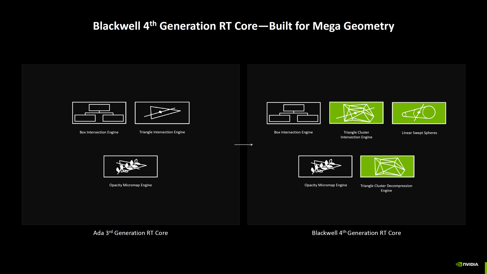
cores include a triangle cluster intersection engine designed specifically for handling mega geometry
Ray Tracing on Blackwell is expected to require 25 percent less graphics card memory than Ada Lovelace
 
Can't say that this "tech deep dive" is very "tech" or "deep". A proper whitepaper would be nice.
Also +30-40% seem to be confirmed now. 5080 will likely end up being slower than 4090 in direct comparisons - unless the new DLSS model would run a lot better on Blackwell leading to some unexpected gains there.
 
Do we know if Blackwell has Level 5 RT now?

Level 5 – Coherent BVH Processing with Scene Hierarchy Generator in Hardware.

12-1080.40ac43d3.png
 
Can't say that this "tech deep dive" is very "tech" or "deep". A proper whitepaper would be nice.
Also +30-40% seem to be confirmed now. 5080 will likely end up being slower than 4090 in direct comparisons - unless the new DLSS model would run a lot better on Blackwell leading to some unexpected gains there.
I don't think we get one. Just look at Datacenter Blackwell and the terribly presentation at hot chips. It's just a basic architecture overview. Nvidia stopped showing real architecute details with Blackwell. It seems like arrogance is starting to win at Nvidia everywhere.
 
@Man from Atlantis That's a pretty big change for the SM. Really looking forward to reading this. Curious of the int32 increase is going to mean anything interesting for performance. My expectation is it won't.

Well Nvidia made a big deal out of saying that INT32 isn’t as important as FP32 to graphics performance. No idea why they’re reversing course now. Maybe it helps more with AI workloads?
 
Can't say that this "tech deep dive" is very "tech" or "deep". A proper whitepaper would be nice.
Also +30-40% seem to be confirmed now. 5080 will likely end up being slower than 4090 in direct comparisons - unless the new DLSS model would run a lot better on Blackwell leading to some unexpected gains there.

Nvidia’s white papers don’t go into much more detail than we’re seeing on these slides. Their CUDA programming guides are slightly better but they haven’t released one for Blackwell.

Anyone else find it strange that there’s zero mention of L2 cache size and capability after they hyped up Ada L2? This really feels like a coasting generation hardware wise. All the fun stuff is in software.
 
Well Nvidia made a big deal out of saying that INT32 isn’t as important as FP32 to graphics performance. No idea why they’re reversing course now. Maybe it helps more with AI workloads?

Kind of wondering if it has something to do with simplifying the SM to improve scheduling of work. You have shader execution reordering and this AMP processor to help schedule ai workloads, and maybe it's just easier to do all of this if the compute resources are all the same.
 
Nvidia’s white papers don’t go into much more detail than we’re seeing on these slides. Their CUDA programming guides are slightly better but they haven’t released one for Blackwell.

Anyone else find it strange that there’s zero mention of L2 cache size and capability after they hyped up Ada L2? This really feels like a coasting generation hardware wise. All the fun stuff is in software.
Judging by the die sizes of GB203/205 in comparison to AD103/104, it seems Nvidia has kept the same L2 cache size.
 
Judging by the die sizes of GB203/205 in comparison to AD103/104, it seems Nvidia has kept the same L2 cache size.

If those die sizes are accurate then Nvidia somehow managed to cram fatter SMs and 4 more of them into the same area. I would be surprised if they didn’t sacrifice L2 to make room and lean more heavily on GDDR7.
 
nVidia said to the press that FP/INT can run concurrently. But no information about the ratio.
Honestly this could mean a lot of things. Concurrently on a chip in the same clock? On an SM which has several SIMDs for that? On one SM partition out of four which they've shown as "SM" in Blackwell to Ada comparison for some reason? Or maybe they are talking about warps which are "in flight" on an SM?
 
So consumer Ada and Blackwell are manufactured on the same 4N node .. explains the modest increases in performance. Not going for N4P (+22% energy efficiency and +6% density) is a strategic choice it seems, as B200 is manufactured on N4P. NVIDIA clearly prioritized the best node for their best data center chip.
Makes me hope and expect RTX 50 will be a short lived gen with no Super 3GB Module refresh and move to RTX 60 Q4 of next year basically a Maxwell to Pascal life cycle (Sep 2024 > May 2026 which was 20 months). Especially if AMD tries to go with UDNA 1st Gen earlier next year (Say Computex annoucement?). I mean 3GB Modules mean 15 (if they 160-bit cut down buses)-24GB becomes the "norm" for gamers.
 
Makes me hope and expect RTX 50 will be a short lived gen with no Super 3GB Module refresh and move to RTX 60 Q4 of next year basically a Maxwell to Pascal life cycle (Sep 2024 > May 2026 which was 20 months). Especially if AMD tries to go with UDNA 1st Gen earlier next year (Say Computex annoucement?). I mean 3GB Modules mean 15 (if they 160-bit cut down buses)-24GB becomes the "norm" for gamers.
Is there a reason IHVs have mostly avoided odd numbers of memory channels? Are they better in pairs or something?
 
Not that I know offrom what's been publicly disclosed.

But IHVs also don't often cut down memory channels in terms of product configuration. I'd wager it's sometimes done here just for some product segmentation as the likely a large factor.

If you mean in design I'd assume it's likely simpler and more optimal from a layout perspective given where the memory controllers/PHYs are located and spaced around the edges of the chip.

This is speculative but if you look at Nvidia's creator slide for RTX 50xx it kind of gives some insight in terms of where certain memory cut off points are going to be for segmentation reasons.
 
Back
Top