DegustatoR
Legend
Makes sense I guess.I don't know of any new docs. FP32 does not need to double - and I am not aware of such a thing. But in Ada, only one of each SIMD16 pairs was combined INT32/FP32, the other one was FP32-only.
Follow along with the video below to see how to install our site as a web app on your home screen.
Note: This feature may not be available in some browsers.
Makes sense I guess.I don't know of any new docs. FP32 does not need to double - and I am not aware of such a thing. But in Ada, only one of each SIMD16 pairs was combined INT32/FP32, the other one was FP32-only.
That's just the usual pass thru cooling right? A bliss for cases like fractal ridge, but a nightmare for sandwich cases like nr200p
On the opposite it may well be a requirement to cool it with a small 2-slot cooler as it allows both fans to blow through the fin stacks.it's amazing they can cool 575W from such a thing
I'm guessing the evolution is -
Pascal-> FP32/INT32
Turing -> FP32 + INT32
Ampere (Ada)-> FP32 + FP32/INT32
Blackwell-> FP32/INT32 + FP32/INT32
On the opposite it may well be a requirement to cool it with a small 2-slot cooler as it allows both fans to blow through the fin stacks.
AIB models so far seem to be your usual 3-4 slot monstrosities.
Do you think the AIB models will be more effective? TBH I don't know if it's safe for the card to draw >600W unless it has 2 power connectors, so assuming NVIDIA's cooler is sufficient for 575W I don't see what purpose making it huge would serve. I get freaked out having such a heavy thing hanging off my PCIe slot, especially when transporting my PC.On the opposite it may well be a requirement to cool it with a small 2-slot cooler as it allows both fans to blow through the fin stacks.
AIB models so far seem to be your usual 3-4 slot monstrosities.
They might be. We'll have to wait for reviews to know that.Do you think the AIB models will be more effective?
So Pascal got it right the first time around? Not sure what difference there is between 1 32-wide SIMD that can do FP32/INT32 and 2 16-wide SIMDs that can do FP32/INT32.
Do you think the AIB models will be more effective? TBH I don't know if it's safe for the card to draw >600W unless it has 2 power connectors, so assuming NVIDIA's cooler is sufficient for 575W I don't see what purpose making it huge would serve. I get freaked out having such a heavy thing hanging off my PCIe slot, especially when transporting my PC.

Unfortunately, the FP32 / INT32 split is an oversimplification of how the HW actually works. There are a bunch of execution ports and on GA102 & newer HW, the typical operations are really split into 3 pipelines: FMAHeavy (FP32 FMA/FMUL/FADD and 32x32 integer multiply-add), FMALite (FP32 FMA/FMUL/FADD only), and INT (integer add, logic ops, *and* floating point comparison including FP32 min/max etc...). Each of the 4 SM sub-cores can only issue 1 instruction per clock (with each of those execution pipelines taking 2 cycles minimum to execute any instruction, you can never issue to the same pipeline two cycles in a row given the 16-wide ALUs with 32-wide warps) so it is impossible to saturate all 3 pipelines simultaneously.I'm guessing the evolution is -
Pascal-> FP32/INT32
Turing -> FP32 + INT32
Ampere (Ada)-> FP32 + FP32/INT32
Blackwell-> FP32/INT32 + FP32/INT32

When was the last architecture in which instruction issue and the ISA was substantially improved? Turing?Unfortunately, the FP32 / INT32 split is an oversimplification of how the HW actually works. There are a bunch of execution ports and on GA102 & newer HW, the typical operations are really split into 3 pipelines: FMAHeavy (FP32 FMA/FMUL/FADD and 32x32 integer multiply-add), FMALite (FP32 FMA/FMUL/FADD only), and INT (integer add, logic ops, *and* floating point comparison including FP32 min/max etc...). Each of the 4 SM sub-cores can only issue 1 instruction per clock (with each of those execution pipelines taking 2 cycles minimum to execute any instruction, you can never issue to the same pipeline two cycles in a row given the 16-wide ALUs with 32-wide warps) so it is impossible to saturate all 3 pipelines simultaneously.
The HW is limited by schedule/fetch/decode/issue logic of 1/clk before even considering that this 1/clk also includes all control/branching/special function/memory instructions... of course, in practice, you might be limited by register file bandwidth or other bottlenecks before being limited by the 1/clk rate, but I believe that rate is indeed a fairly common bottleneck.
It's impossible to say exactly what NVIDIA has done here before we get access to the SASS disassembly & can write microbenchmarks, but for example there's no good reason for them to double the 32x32 multiply-add pipeline; actually now that they have the TMA, even 1/2 rate 32x32 IMAD feels very excessive to me (AMD is 1/4 rate iirc) but maybe it still makes sense to keep it for the majority of workloads that do not use TMA...
Doubling the "integer" pipe (which really isn't just integer - e.g. FP32 min/max) would be nice, but what I really want to see is an increase to the instruction fetch/decode rate, and ideally something bettere than their extremely low density 128-bit fixed length ISA ... Hopper has proven low code density doesn't really matter for matrix multiplication & deep learning especially if you just use much longer asynchronous TMA & WGMMA instructions (instruction decoder is actually idle a lot of the time for Hopper matrix multiplication kernels!) but it's still an obvious weakness of the architecture, including for things like raytracing where instruction cache misses are common and NVIDIA's very aggressive prefetching won't work as well (or might even have to be disabled completely for certain workloads afaik).
Volta was the last "completely new ISA" - every generation since then has mostly "just" been (significant!) additions on top of the same baseline ISA, e.g. Turing uniform registers is a pretty big change but the existing Volta instructions didn't change much. NVIDIA doesn't explain what any SASS instruction actually does, but they do list them in their entirety(?) on this page, and you can see how Hopper is roughly a superset of Volta: https://docs.nvidia.com/cuda/cuda-binary-utilities/index.htmlWhen was the last architecture in which instruction issue and the ISA was substantially improved? Turing?
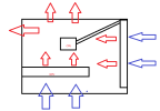
Aren't the PSU shrouds usually on the bottom? Where is the PSU going with this flow? Moved up front or really wide case with side mount?I can't remember what the 12v connector is called, but I think it handles 600W on its own, and then you have the pcie5.0 power delivery. Honestly, I think dual flow-through should probably cool a lot better. It's basically designed like a 240mm radiator, but with a small gpu pcb stuck directly in the middle. We'll have to wait and see.
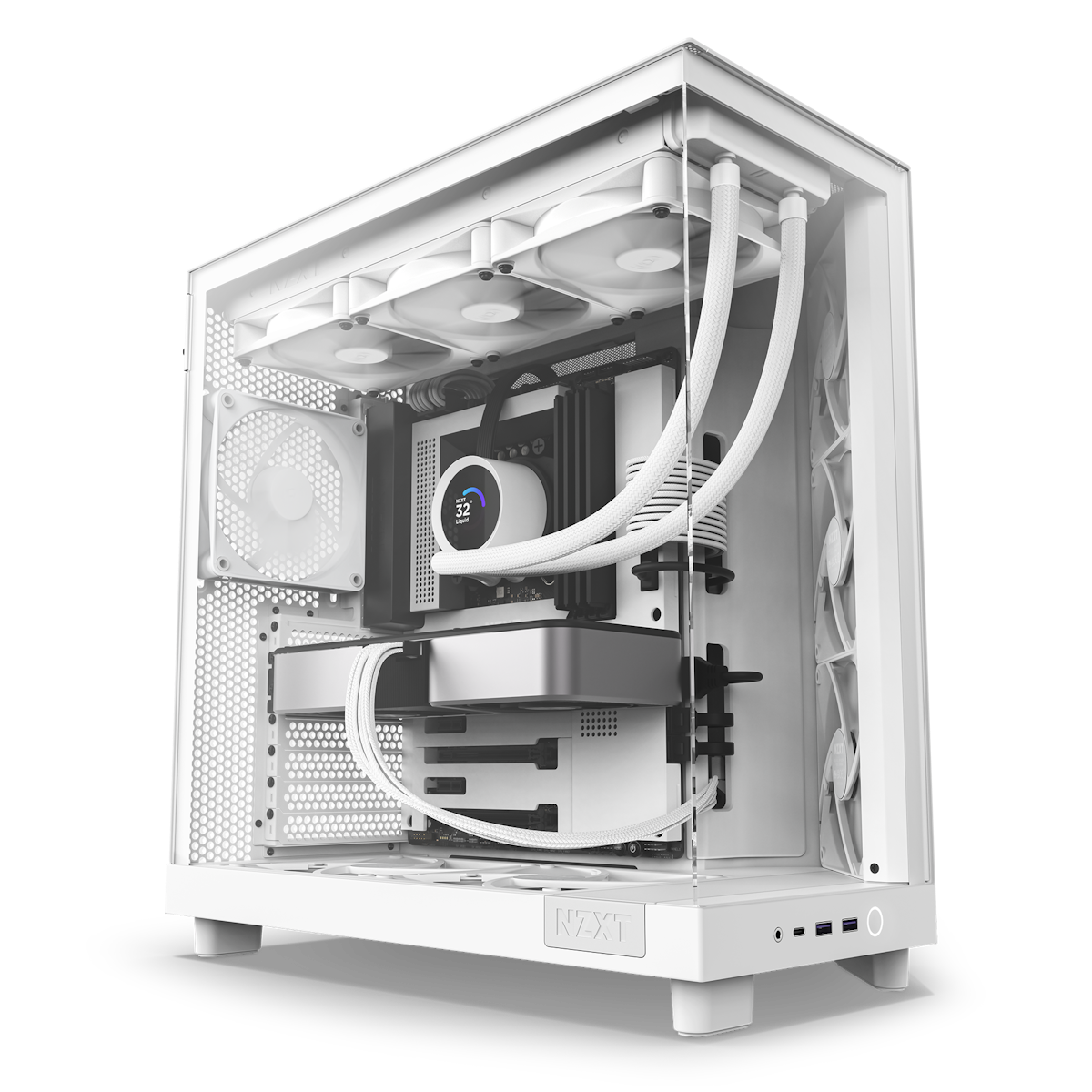
There are a lot of new cases that have fans that pull in air from the bottom, which is perfect for this flow through gpu design. I'd stick an aio rad for the cpu in the front of the case as an intake, have bottom intake fans for the gpu and then have exhaust fans in the back and top.
View attachment 12826
Aren't the PSU shrouds usually on the bottom? Where is the PSU going with this flow? Moved up front or really wide case with side mount?

