Next Generation Hardware Speculation with a Technical Spin [pre E3 2019]

Status
Not open for further replies.
More food for thought: AMD's GPU development history

AMD's Top-end Single GPU Video Card
2012 - 7970 - 28nm - 3.79 TF
2013 - R9 290X - 28nm - 5.63 TF
2015 - Fury X - 28nm - 8.6 TF
2017 - Vega 64 (Air) @ Boost Clock - 14nm - 12.67 TF
2019 - Radeon VII @ Boost Clock - 7nm - 13.82 TF

Consoles based on AMD GPU
2013 - PS4 - 28nm -1.8 TF
2016 - PS4 Pro - 14nm - 4.2 TF
2017 - Xbox One X - 14nm - 6 TF

A console based on a SoC containing an AMD GPU has never had more than 1/2 the total TF capability of the top-end GPU from AMD at any time during this period. Keep that in mind when setting your expectations for the performance of next-gen consoles.

I would like to know what would be the power consumption when Vega 64 is clocked at a more reasonable frequency (let's 1.2 in case 64cu (4096sp) enabled or 1.3Ghz -> 60cu (3840sp) enabled). Both of these configurations would allow reaching 10TF. I feel these boost clocks seem to draw an abnormal amount of juice of the cards.
 
It is grim and those numbers are a good grounding point for this situation. I do feel like they paint a little pessimistic scenario though. The increase in those numbers doesn't look that bad until the
Radeon 7. AMD has hit a pretty major power wall already with the Vega 64 pushing 300W and the process shrink to 7nm didn't bring them all that much on that similar Vega 20 design. However those chips have been pushed wayyy past their sweet spots due to the competitive landscape. Vega 56 gives over 10TF at 225W and people have been getting pretty good power savings on Vega 64 by sacrificing little bit of performance. I think there is reason to believe that a console chip could be closer to PC teraflops than before due to the hard power wall.

If you look at the Vega 64 review by Techpowerup, you can see that using a power save bios that limits the power draw to around 200W, they are still getting 92% of the performance.

https://www.techpowerup.com/reviews/AMD/Radeon_RX_Vega_64/29.html

https://www.techpowerup.com/reviews/AMD/Radeon_RX_Vega_64/31.html


Also Launch PS4 with 1.84TF on 28nm consumed around 140W, PS4 Pro consumes around the same watts on 16nm with 4.2TF and One X only increased this to around 170W with 6TF. That is great scaling with just one major node difference. Better AMD design with 7nm should make it easy(ish) to push past 10TF, even if the wall hits hard a little further. The base and possible premium SKUs throws a little wrench there, but at least the higher SKUs should get there.
Let's hope the rumors of Navi arch holding 1.6 x of logic in the same die space as Vega 14nm is still true, that would translate to a 20 tf gpu effectively. But that would still at best give us a 10 tf console going by the trend. Weak sauce it is but better than nothing I guess.
 
What’s to stop them from a Kaby Lake G type solution? The IO can all be on the GPU chiplet.
AMD could save on the costs of interposer if they used Intel's EMIB (Embedded Multi-Die Interconnect Bridge) approach.

This would need a bigger package though, as all IO contacts must be very closely aligned - resulting in an elongated die on the sides where EMIB connections are engaged.

It's also an Intel exclusive so far, with no roadmaps from AMD or other chip makers.
 
Last edited:
I had some counter arguments in the other thread, I'm not going to copy paste them, but I will repeat that Vega 7 is not a good base for these calculations. It has too much baggage compared to a true gaming only design and is a shrink from the old 14nm process. TSMCs 7nm should offer close to 3x the amount of transistors per mm2 compared to their 16nm process, which is quite similar to the Glofo 14nm. While I'm not quite expecting that type of increase in transistors, the math that there is enough room for 56CUs when when the Xbox One X already has 44 on chip on 16nm is quite flawed imo.
I pretty much agree with this, but the transistor density of Vega 20 still gave me some pause, so I dug into it a bit.
Going by the otherwise identical Apple A9 chips, Samsung 14nm was denser than TSMC 16nm at that point, to the tune of (96mm2(S)/104.5mm2(T)=0.92) yielding a transistor density of 20.8million/mm2(S) or 19.1million/mm2(T).
The A12 at 7nm TSMC has a transistor density of 6.9E9/83.3mm2=82.8million/mm2 and for the A12x it's 1.0E10/122=82.0million/mm2.
That's fantastic scaling by the way.
However, when we look at Vega 10 at 14nm GloFo vs. VEGA 20 on 7nm, we find that VEGA 10 has a transistor density of 12.5E9/484mm2=25.8million/mm2 versus the VEGA 20 at 13.3E9/331mm2=40.2million/mm2.
Even taking into account that GloFo 14nm may well have been a bit denser than TSMC 16nm, the density scaling still raises some concerns.
I/O circuitry doesn't scale as well as logic and SRAM, which in itself would pose limits, and doubly so for Vega 20 with its twice as wide 4096-bit wide interface.
Also, higher performance circuitry use lithography that is less dense for a variety of reasons. Just how much of an impact that has is difficult to assess from a sample of one. (Actually, a cursory analysis of the 7nm Ryzen die implies that density scaling has been quite modest, but that's worse data than VEGA20 at this point).

What this boils down to basically is some caution in making too optimistic assumptions about what density 7nm console chips will demonstrate, after Vega 20 and what little can be gleaned from the 7nm Ryzen die.
So - same opinion, but with numbers. ;-)

Edit: For reference Scorpio density is 7E9/359mm2=19.5million/mm2
 
Last edited:
Yeah Apple has been able to put pretty crazy number of transistors in their SOCs on 7nm, where as the Vega 20 increase is significantly less, it still offers over 2X transistors per mm2 over the One X and even though I don't believe that 40M per mm2 to be the ceiling for the next gen SOCs, I think it's clear it's not the transistors or the die size that is going to be the limiting factor, but the power consumption. They will have room to put too much in there imo, unless Navi is a miracle, and I don't believe it will be. Hopefully it will give us that 10-12TF though :)
 
Yeah Apple has been able to put pretty crazy number of transistors in their SOCs on 7nm, where as the Vega 20 increase is significantly less, it still offers over 2X transistors per mm2 over the One X and even though I don't believe that 40M per mm2 to be the ceiling for the next gen SOCs, I think it's clear it's not the transistors or the die size that is going to be the limiting factor, but the power consumption. They will have room to put too much in there imo, unless Navi is a miracle, and I don't believe it will be. Hopefully it will give us that 10-12TF though :)
I tend to regard the Vega 20 as a lower bound for density on 7nm, when it comes to predicting the console APUs. Using Vega 10 as a base and targeting professional applications, Vega 20 had every reason to make choices that prioritizes clock scaling over density. That is not the case for a relatively large console APU that targets mass market pricing at high volume. Improvements in density makes a real difference to the bottom line under those circumstances.

So, however, does simply designing a smaller chip.
 
Yeah Apple has been able to put pretty crazy number of transistors in their SOCs on 7nm, where as the Vega 20 increase is significantly less, it still offers over 2X transistors per mm2 over the One X and even though I don't believe that 40M per mm2 to be the ceiling for the next gen SOCs, I think it's clear it's not the transistors or the die size that is going to be the limiting factor, but the power consumption. They will have room to put too much in there imo, unless Navi is a miracle, and I don't believe it will be. Hopefully it will give us that 10-12TF though :)
Apple is using the 7nm process optimized for mobile/SoC usage. Only 6T versus 7.5T and much higher transistor density because the power density is much lower.

AMD could save on the costs of interposer if they used Intel's EMIB (Embedded Multi-Die Interconnect Bridge) approach.

This would need a bigger package though, as all IO contacts must be very closely aligned - resulting in an elongated die on the sides where EMIB connections are engaged.

It's also an Intel exclusive so far, with no roadmaps from AMD or other chip makers.

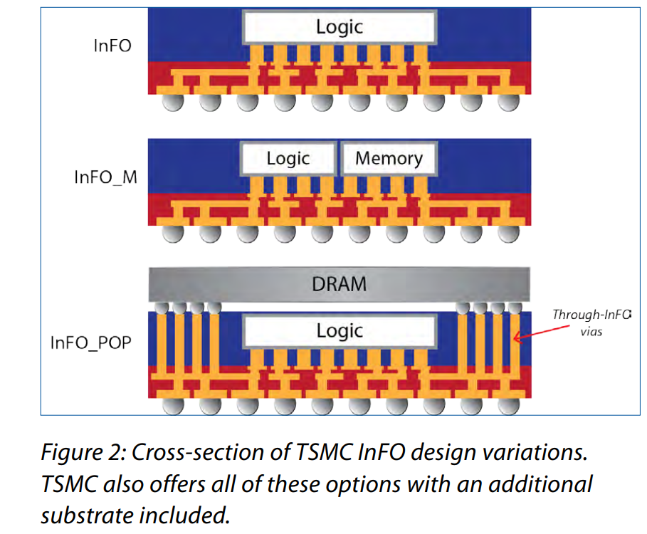
EMIB is interesting but I bet the cost advantages will dwindle over time. As for AMD, word is that TSMC will get EPYC production using their CoWoS process. TSMC has a bunch of variants of InFO on the way - some aimed at HBM and others for true 3D stacking. The packaging landscape could be very different by the time consoles launch.

https://www.eetimes.com/document.asp?doc_id=1333244&page_number=3

Now that TSMC has established its 2.5-D CoWoS package in GPUs and other processors and its wafer-level fan-out InFO in smartphone chips, it is expanding both offerings and adding others.

CoWoS chips will have options for silicon interposers up to twice a reticle’s size, apparently stitched in the field, starting early next year. Versions with 130-micron bump pitch will be qualified this year.

The InFO technique is getting four cousins. Info-MS, for memory substrate, packs an SoC and HBM on a 1x reticle substrate with a 2 x 2-micron redistribution layer and will be qualified in September.

InFO-oS has a backside RDL pitch better matched to DRAM and is ready now. A multi-stacking option called MUST puts one or two chips on top of another larger one linked through an interposer at the base of the stack.

Finally, InFO-AIP stands for antenna-in-package, sporting a 10% smaller form factor and 40% higher gain. It targets designs such as front-end modules for 5G basebands.

But that’s not all. TSMC introduced two wholly new packaging options.

A wafer-on-wafer pack (WoW) directly bonds up to three dice. It was released last week, but users need to ensure that their EDA flows support the bonding technique. It will get EMI support in June.

Finally, the foundry roughly described something that it called system-on-integrated-chips (SoICs) using less than 10-micron interconnects to link two dice, but details are still sketchy for the technique to be released sometime next year. It targets apps from mobile to high-performance computing and can connect dice made in different nodes, suggesting it may be a form of system-in-package.

infoms.png


http://itersnews.com/wp-content/uploads/experts/2017/02/105162mentorpaper_98612.pdf

I pretty much agree with this, but the transistor density of Vega 20 still gave me some pause, so I dug into it a bit.
Going by the otherwise identical Apple A9 chips, Samsung 14nm was denser than TSMC 16nm at that point, to the tune of (96mm2(S)/104.5mm2(T)=0.92) yielding a transistor density of 20.8million/mm2(S) or 19.1million/mm2(T).
The A12 at 7nm TSMC has a transistor density of 6.9E9/83.3mm2=82.8million/mm2 and for the A12x it's 1.0E10/122=82.0million/mm2.
That's fantastic scaling by the way.
However, when we look at Vega 10 at 14nm GloFo vs. VEGA 20 on 7nm, we find that VEGA 10 has a transistor density of 12.5E9/484mm2=25.8million/mm2 versus the VEGA 20 at 13.3E9/331mm2=40.2million/mm2.
Even taking into account that GloFo 14nm may well have been a bit denser than TSMC 16nm, the density scaling still raises some concerns.
I/O circuitry doesn't scale as well as logic and SRAM, which in itself would pose limits, and doubly so for Vega 20 with its twice as wide 4096-bit wide interface.
Also, higher performance circuitry use lithography that is less dense for a variety of reasons. Just how much of an impact that has is difficult to assess from a sample of one. (Actually, a cursory analysis of the 7nm Ryzen die implies that density scaling has been quite modest, but that's worse data than VEGA20 at this point).

What this boils down to basically is some caution in making too optimistic assumptions about what density 7nm console chips will demonstrate, after Vega 20 and what little can be gleaned from the 7nm Ryzen die.
So - same opinion, but with numbers. ;-)

Edit: For reference Scorpio density is 7E9/359mm2=19.5million/mm2
A zen CCX has 1.4B transistors in a 44mm^2 area, and that has 8MB L3. Let's assume all the I/O can go on the IO die, so a Zen 2 chiplet would literally just be two CCXs. We start with 2.8B trasnsistors in a 70-80mm^2 die. However, we know L3 cache has doubled, so that's an additional 16 * (2^20 for MB) * (8 bits per byte) * (6 transistors per bit) = 805M transistors. 1.4B in 44mm^2 vs. 3.6B in (70-80mm^2). That's somewhere in the range of a 41-61% density increase. However, that assumes no core growth for Zen 2, which is not at all realistic given the doubling of FP paths and beefing up of the front-end of the processor. I would confidently venture we're looking at over a 70% increase in transistor density, which is indeed a far cry from the 70% area scaling TSMC claims for (what I presume is mobile process comparisons) 16FF to 7FF. The Apple numbers you cite are much closer to the 3.33x density increase advertised (actually beating it). The Zen 2 numbers are somewhat consistent with what we already known from MI25 and MI60 though. That die only shrunk 35%, but that number is pessimistic given the 0.7B transistor growth and poor memory controller scaling (and doubling).
 
Last edited:
I'd think they provided for this capability during the principal development stage rather than postpone it to a potentially risky respin on a new node.
The fact that none of the Vega 10 -based Pro and Instinct cards have 1:2 DP, it's highly unlikely the chip would have the capability for it.
 
At this point my expectation for the performance level of next-gen console GPUs is 10-12 TF with efficiency improvements to the architecture leading to a better utilization of those resources. If a leak hasn't happened by the time Navi comes out, I'll adjust if necessary based on the characteristics of GPUs based on that architecture.
 
I would confidently venture we're looking at over a 70% increase in transistor density, which is indeed a far cry from the 70% area scaling TSMC claims for (what I presume is mobile process comparisons) 16FF to 7FF. The Apple numbers you cite are much closer to the 3.33x density increase advertised (actually beating it). The Zen 2 numbers are somewhat consistent with what we already known from MI25 and MI60 though. That die only shrunk 35%, but that number is pessimistic given the 0.7B transistor growth and poor memory controller scaling (and doubling).

I wonder if at least partly the reason for the Zen 2 scaling is that the removal of heat could really start to be an issue with a smaller physical size. The 7nm die is already very small now that the I/O has been moved to a separate die and some of the configurations will have quite high power consumption. Perhaps they are tapping mainly to the speed increase instead of area scaling benefits of the 7nm process for that reason?
 
The thing that confuses me about these sorts of leaks is why would any single developer have knowledge of the progress and launch plans of other developers/publishers? As soon as I see a list of titles in one of these, my BS detector goes off. Am I right to think this?
 
Last edited:
I wonder if at least partly the reason for the Zen 2 scaling is that the removal of heat could really start to be an issue with a smaller physical size. The 7nm die is already very small now that the I/O has been moved to a separate die and some of the configurations will have quite high power consumption. Perhaps they are tapping mainly to the speed increase instead of area scaling benefits of the 7nm process for that reason?
I think there could be truth to that. Just having the high switchers focused with no less active portions to heat spread could be an issue.

On the other side of the coin, apparently Zen 2 can hit 3.7GHz base clock at 65W TDP, 0.5GHz higher than the Zen+ equivalent at the same TDP. That’s pretty good clock growth and much better than what we’ve seen in mobile.
 
Could be some bloat for the L3 blocks. If you look at the Zen 1 die shot, there's quite a bit of un-cache area for the entire block, and if you compare that Raven Ridge's half-L3, there really wasn't that much savings in area considering.

There will be some bloat from the Infinity Fabric as well.

edit:

Zen 1 CCX = 44mm^2, 8MB L3 ~16mm^2
Raven Ridge = ~41mm^2, half-L3, but the area devoted to it is still ~12mm^2, probably owing to the overhead for the interconnect/wiring.
 
Last edited:
TSMC will get EPYC production using their CoWoS process. TSMC has a bunch of variants of InFO on the way - some aimed at HBM and others for true 3D stacking. The packaging landscape could be very different by the time consoles launch.
A stacked TIV package integrating IO die and HBM sure looks promising, but the technology has to be available for volume production well in advance to the actual launch - that is, by end of 2019. InFO has only been used for high-density packaging of mobile parts so far - it's not clear if it could be scaled to high-power desktop chips.

I would confidently venture we're looking at over a 70% increase in transistor density, which is indeed a far cry from the 70% area scaling TSMC claims for (what I presume is mobile process comparisons) 16FF to 7FF. The Apple numbers you cite are much closer to the 3.33x density increase advertised (actually beating it).
I wonder if at least partly the reason for the Zen 2 scaling is that the removal of heat could really start to be an issue with a smaller physical size.
Sure it could. We are approaching atom-scale resolutions where leakage currents could affect signal integrity and power consumption - so a 300 W desktop GPU and a 100 W desktop CPU would scale differently comparing to a 5 W mobile APU.

The fact that none of the Vega 10 -based Pro and Instinct cards have 1:2 DP, it's highly unlikely the chip would have the capability for it.
They said "configurable DP rate" in the promotional materials and I assume that means a higher rate for professional parts - as to why it was never enabled for Vega10, could be some implementation bug.
 
Last edited:
A TSV package integrating IO die and HBM sure looks promising, but the technology has be available for volume production well in advance to the actual launch - that is, by end of 2019. InFO has only been used for high-density packaging of mobile parts so far - it's not clear if it could be scaled to high-power desktop chips.


Sure it could. We are approaching atom-scale resolutions where leakage currents could affect signal integrity and power consumption - so a 300 W desktop GPU and a 100 W desktop CPU would scale differently comparing to a 5 W mobile APU.

They said "configurable DP rate" in the promotional materials and I assume that means a higher rate for professional parts - as to why it was never enabled for Vega10, could be some implementation bug.
Theoretically it should help HPC class chips. The original InFO was touted as having a 10% thermal advantage. This presumed the technique can handle the higher thermal stresses HPC would demand.

Compared to existing package scheme, TSMC's InFO can bring greater-than-20% reduction in overall package thickness, 20% speed gain in performance and 10% better in thermal performance for power dissipation.

https://www.tsmc.com/uploadfile/ir/quarterly/2015/3C2bO/E/TSMC 3Q15 transcript.pdf
 
Last edited:
Very funny fake leak of PS5 on reddit Hilarious... I don't want to spoil it
How ashamed should I feel for thinking it was all believable until he said half of the 16GB GDDR6 would be for the OS alone?


A TSV package integrating IO die and HBM sure looks promising, but the technology has be available for volume production well in advance to the actual launch - that is, by end of 2019. InFO has only been used for high-density packaging of mobile parts so far - it's not clear if it could be scaled to high-power desktop chips.
Then again, that Sony patent about a heatsink that would cross the PCB to make contact with the die on the bottom would be a nice hypothetical fit for an InFO_PoP.
 
How ashamed should I feel for thinking it was all believable until he said half of the 16GB GDDR6 would be for the OS alone?

The description of how the oled panel would work given what the dimensions of it would be to fit in what was described as a similar form factor to a DS4 was ludicrous. Picture trying to play PS5 games on a screen the size of the one in one of those Tiger LCD games.
 
PSVR2 for $100 RETAIL ...
A 6TB SSD included in $400 console ...
 
Status
Not open for further replies.
Back
Top