Those dice are so smol they have to be really cheap anyway.
So much so compared to increasing the main die with their area..
Looking at die costs and excluding the extra cost of packaging and any extra wafer prep for the interconnect...
MCDs are ~$4 each, <$5. Assuming +95% yield.
GCD are ~$90-$95 each, <$100. Assuming ~90% yield.
If it is on an interposer, add another ~$10.
2nd Edit- Forgot the slide deck said they are using Elevated Fanout Bridge for the interconnect, so supposedly "standard flipchip processing."
~525mm2 on 5nm ~$170-$190 each, <$200. Assuming ~85% yield.
So say ~$130 for Navi31 which would be ~25-30% cheaper than if they went monolithic, based on my rough estimations.
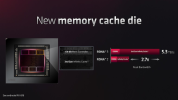
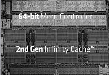
Edit- Also found the apparent ratio of the MCD interesting, looking at the attached slide and assuming it is somewhat accurate.
Using my very, very rough estimates...
Interconnect on the side closest to the GCD appears to be ~10% the area, ~3.7mm2.
64bit MC appears to be ~25% the area, ~9mm2.
The 16MB of 2nd Gen IC appears to be ~66% the area, ~24.4mm2.
The CPU V-cache is 64MB @ 41mm2. So v-cache ~10mm2 per 16MB and 16MB of GPU IC is more than twice the size?
Is the size difference due to the speed necessary for GPU cache or is there extra logic involved with GPU IC?