
Benetanegia
Regular
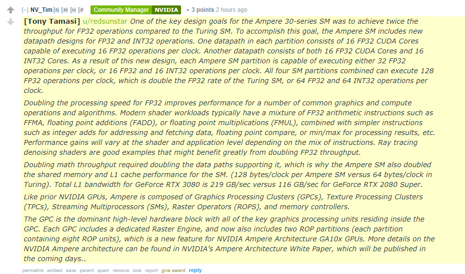
nVidia explains how they have archived 2x FP32 throughput, enjoy:
Heh! So we nailed it several months ago.
nVidia explains how they have archived 2x FP32 throughput, enjoy:
Good that it's finally in the open.nVidia explains how they have archived 2x FP32 throughput, enjoy:
")

Not sure why doubling cache bandwidth was needed tho? In Turing there were 2 datapaths too, from what was told, one for FP, the other for INT, with Ampere the INT one just gets shared with FP, right?
I guess in Turing INT datapath was like a second rate bandwidth consumer because it would be idling more time than not anyway? And now that the seccond datapath will consume at all times, a adoubling ir required? Any thoughts?
What does this actually mean? Instead of a crossbar for data transfers between the GPCs and ROPs, that traffic now has to route through GPCs?
"Each GPC includes a dedicated Raster Engine, and now also includes two ROP partitions (each partition containing eight ROP units), which is a new feature for NVIDIA Ampere Architecture GA10x GPUs."
Also, how is the combined FP32/INT32 pipeline any different to Pascal/Maxwell/Kepler etc? This doesn't sound like a new thing.
Doing a bit of ROP math assuming GA102 has 84SMs total.
96 ROPs = 6 GPCs = 14 SMs per GPC or
192 ROPs = 12 GPCs = 7 SMs per GPC.
If it's the latter that's going to be a chunky increase in raw rasterization throughput.
Turing 1 FP32 + 1 INT32
Ampere 1 FP32 + 1 (FP32 or INT32)
So Ampere can have double the FP32 rate of Turing, but when INT32 is mixed it is the same as Turing. So mileage will vary based on workload.
In Turing, there was a set of FP32 ALUs and a set of INT32 ALUs, each could work in parallel. With Ampere, the INT32-set was expanded to be able to do FP32 as well. That's my take of it.
GA102, judging from the die shot, should be at 7 GPCs, so 7x8x2=112 ROPs with full config. Probably, Nvidia can enable/disable ROPs independently from memory partitions now.
I wonder why no one's talking about GA104 already...
This seems like a logical option but I wonder if having them separate in h/w would actually be _less_ complex than having one SIMD capable of FP32+INT32.With Ampere, the INT32-set was expanded to be able to do FP32 as well.
GA102, judging from the die shot, should be at 7 GPCs, so 7x8x2=112 ROPs with full config. Probably, Nvidia can enable/disable ROPs independently from memory partitions now.
That's what Tamasi's answer sounds like to me, yeah.Oh, that's interesting. It must mean they decoupled ROPs from the memory controllers so the number of ROPs is no longer determined by bus width.
You mean like FP32+FP32+INT32? I would have approached it the other way around: have both blocks be able to do FP32 or INT32. Both would be a little bit bigger, but you had more opportunities to schedule.This seems like a logical option but I wonder if having them separate in h/w would actually be _less_ complex than having one SIMD capable of FP32+INT32.
Yeah. Three 16-wide SIMDs: FP32+FP32+INT32. This would explain the reasoning behind the extension of data paths at least as otherwise you'd have the same 64 bits going to the same two SIMDs with one or two of them being capable of FP32+INT32 now.You mean like FP32+FP32+INT32? I would have approached it the other way around: have both blocks be able to do FP32 or INT32. Both would be a little bit bigger, but you had more opportunities to schedule.
Also, how is the combined FP32/INT32 pipeline any different to Pascal/Maxwell/Kepler etc? This doesn't sound like a new thing.
I think the difference is in power gating granularity. Being able to switch off part of it versus only being able to switch the entire thing off when doing nothing. Specifically switching off the INT SIMDs when only doing FP. Because iirc from some (twitter?) posts at the time, the FP unit actually only takes care of the most relevant (more used) FP instructions, while the so called INT units also do some fringe less used FP instructions. I suppose this way the FP units become the leaner (less micro-instructions supported), most used unit that is enbled most of the time and the INT units are the fat units that get switched off most of the time.
I prefer the more sober approach.
Goes for every product though, can find alot sober approaches to PS5, AMD, NV, MS if i want to.FP32+[FP32|INT32] is still my go-to choice