AMD: R9xx Speculation

They also forget to tell that someone needs to make a memory controller that works at those speeds fine (which could add to costs). Nvidia had problems to reach 4GHz on the first try :rolleyes:
Well, AMD didn't quite reach 1Ghz with first try (rv770) neither (at least they only needed 1Ghz chips to reach their 900Mhz...) - though maybe they didn't really try as the HD4870 definitely wasn't bandwidth starved. First 40nm gddr5 controller (rv740) had quite low speed too, and that one could have benefited from a bit more, though it was meant to be quite cheap.
In any case, rv870 (as well as rv840) seems to be able to run at 1.25Ghz (the rated maximum of the chips) easily, so I don't think a bit of an increase should be any problem for next gen. Might not quite reach the 1.75Ghz for those 7gbps chips, but who knows if hynix actually can deliver those anyway - something like 1.5Ghz would at least be a 20% improvement.
 
Indeed, my XXX edition 5770 runs at 1300Mhz out-of-the-box.
 
In any case, rv870 (as well as rv840) seems to be able to run at 1.25Ghz (the rated maximum of the chips) easily, so I don't think a bit of an increase should be any problem for next gen. Might not quite reach the 1.75Ghz for those 7gbps chips, but who knows if hynix actually can deliver those anyway - something like 1.5Ghz would at least be a 20% improvement.

Assuming that Charlie has the correct information then even a 20% increase in bandwidth will be enough for a chip refresh especially as it looks like the refresh is along the lines of efficiency rather than outright theoretical performance increases. In that order then the Island chain of chips ought to be more efficient at its use of bandwidth even if the chip is relatively static in terms of execution performance.

One thing I do wonder is if the next chip will infact be larger on the same process due to improvements in the process design and the desire to pack more transistors into the same design or if it will be relatively static in size or even smaller due to a tighter packaging of said transistors.
 
Well, you could always make your controller ECC capable to offset all the erroneous bits in your high speed data transfers! :D

GDDR5 already employs EDC with retry just to maintain reliability at 4-5 GHz. Any additional error detection/correction will be marginal at best. Its really more of a fundamental signal integrity and BER issue at this point.
 
http://www.xbitlabs.com/news/video/..._Different_Suppliers_Hybrid_Architecture.html

I think this article nicely sums up where we are now with the rumours.

Though I don't think Southern Islands is a response to 32nm being aborted by both TSMC and GF, I think it's been there all along, being the 40nm bridge from Evergreen to Northern Islands. Hence my signature.

Jawed

If ati goes with 40 nm for SI, then there is a real chance of nv risking 28nm and landing a KO. Even if they don't have a new process anymore, they still have a new pipeline arch - Charlie seems to suggest that it has been done already though - and nv's GDDR5 MC should have been fixed by that time - it's been more than a year now. Overall, a good chance that the competitive situation will reverse itself.

However, considering TSMC's 40nm track record, 2Q11 seems best bet for 28nm gpu's from both though.
 
If anyone (or anything) has ONE single name for one of the S.I. chips, i'd be very grateful
 
Thinking about it some more I'm starting to question the timing of 32nm. I've realised, contrary to my earlier thoughts, that 32nm might have been treated as a "half node" by TSMC, an optical shrink. But I'm unsure, to be honest, because 40nm was originally a half-node of 45, so 32 would have been a full-node from 45.

In a sense TSMC has shifted its full nodes by half a node downwards (45 became 40nm) and seemingly dropped half-nodes (no 32nm from 40nm). I suppose this depends on whether "half node" is defined by the ability to use an optical shrink, or if it merely reflects steppings that are substantially less than a 2x density increase.

Let's imagine this is the original roadmap, the one that AMD was working to at the end of 2007:

2008Q4 - 40nm - RV740 pipe cleaner - strong evidence this was on roadmap

2009Q3 - 40nm - Evergreen

2010Q2 - 32nm - Southern Islands

2010Q4 - 28nm - SI pipe-cleaner - strong evidence that TSMC was planning for this quarter

2011Q2 - 28nm - Northern Islands

On that basis it would appear that SI has to make do with 40nm, which is a bit of a blow. But not a disaster because, remember, Cypress was planned to be bigger on 40nm, so a SI-refresh of Cypress on 40nm will only be what AMD was originally aiming for, or a little bigger (extra features that were planned for SI anyway - but maybe not all SI features).

As for NVidia, I'll believe they can execute when they do actually execute. NVidia's got things to fix before it can execute. That's not to say that SI hasn't got elements that could break AMD's execution, independent of TSMC's and GF's best efforts to fuck everything up.

I presume AMD will trim SI in light of 32nm's disappearance. The SI pipe-cleaner might be less trimmed.

Jawed
 
If ati goes with 40 nm for SI, then there is a real chance of nv risking 28nm and landing a KO. Even if they don't have a new process anymore, they still have a new pipeline arch - Charlie seems to suggest that it has been done already though - and nv's GDDR5 MC should have been fixed by that time - it's been more than a year now. Overall, a good chance that the competitive situation will reverse itself.

However, considering TSMC's 40nm track record, 2Q11 seems best bet for 28nm gpu's from both though.

I don't think Nvidia can go 28nm like that. Their designs are over-ambitious for a brand new process, and TSMC is particularly bad at complex chips on new cutting edge processes. I would expect AMD to be first with a graphics chip at 28nm, most likely a smaller mainstream chip at Global Foundries.

I doubt it will make a difference to SI. SI will be designed to hit the sweet spot strategy and ship on time with the highest performance on he process available, whilst Nvidia will still be getting the bugs out of the manufacture of the massive top-end Fermi.

TSMC pulled the 28nm ahead by a quarter. A dumb shrink of Fermi might be enough time (and be small enough) to fix the heat/clocks/yields and upstage ati.

GF is ~1Q behind TSMC in process roadmap, according to original 32 nm plans. 28 nm is prolly next year. That does put a bit of strain on the claims that NI wafers were on display @CES2010. ;)

At any rate, it does seem *very* plausible that competitive landscape will be quite different next gen.
 
TSMC pulled the 28nm ahead by a quarter. A dumb shrink of Fermi might be enough time (and be small enough) to fix the heat/clocks/yields and upstage ati.
But 28nm at TSMC won't be shrink of 40nm, no?
I thought they switched technology (gate first to gate last or vice versa), so a 28nm chip needs rebuilding, not from scratch but still "dumb shrink" looks impossible. :?:
 
But 28nm at TSMC won't be shrink of 40nm, no?
I thought they switched technology (gate first to gate last or vice versa), so a 28nm chip needs rebuilding, not from scratch but still "dumb shrink" looks impossible. :?:

I am no VLSI expert, but I think the change from gate first->gate last should not be much of a biggie when you are shrinking a chip and trying to fix power/clocks/yields, especially if the logic stays put.
 
TSMC pulled the 28nm ahead by a quarter.
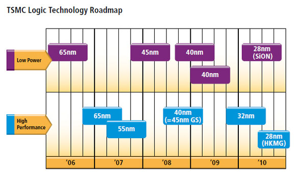
According to TSMC roadmap,its 40nm HP node should be ready at Q3 2008....So why would you think TSMC 28nm node would be on time?

TSMCRoadmap.jpg
 
TSMC pulled the 28nm ahead by a quarter. A dumb shrink of Fermi might be enough time (and be small enough) to fix the heat/clocks/yields and upstage ati.

GF is ~1Q behind TSMC in process roadmap, according to original 32 nm plans. 28 nm is prolly next year. That does put a bit of strain on the claims that NI wafers were on display @CES2010. ;)

At any rate, it does seem *very* plausible that competitive landscape will be quite different next gen.

TSMC just moved 28nm on their schedule - and we know how reliable their roadmaps have been. I wouldn't be surprised if that's a face saving exercise. I'd expect that to slip by a minimum of 1-2 quarters. GF on the other hand have already publicly shown unnamed graphics chips wafers.

Can Nvidia do a dumb shrink of Fermi? Isn't a shrink down to the next node going to mean a redesign, especially if TSMC has gone from a gate first to gate last? I think a Fermi shrink is going to be quite a lot more complicated that just a simple shrink of the same design.

Personally, I think the main problem is the design ethos at Nvidia - they keep going for massive chips on new processes that arn't ready for them. Their company culture doesn't seem to be allowing them to change to a different way of thinking. Just look at the trouble ATI had changing their culture to go to the sweet-spot strategy and sort our their execution.

Until Nvidia show they can execute well by actually executing well, there's no reason to wishfully think they will be able to turn things around in a few months while still following the mantra of massive chips on brand new processes.
 
According to TSMC roadmap,its 40nm HP node should be ready at Q3 2008....So why would you think TSMC 28nm node would be on time?

TSMCRoadmap.jpg

I know it's fucked up. BADLY. But I am merely saying that for nv it's worth risking a 28nm shrink around that time. If TSMC delays it, they ofc can't help it. But **IF** it works out, they are in luck.

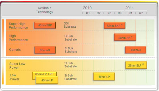
This is the latest I can find on GF.

http://hothardware.com/News/One-Year-Later-GlobalFoundries-Rapidly-Ramping-New-Technologies/


GFSlide3.jpg


32nm processors should ship in volume by the end of 2010.
You believe this one?

PS: that pic was from ~4 years ago. It's useless today.
 
That's a fairly poor article since it doesn't even question the huge gap in 40nm bulk that GF's roadmap paints.

PS: that pic was from ~4 years ago. It's useless today.
It makes a useful baseline for what AMD's plans once were - hence my earlier exposition of SI and NI. Obviously no one believes TSMC's optimism about 28nm.

Jawed
 
最新消息:TSMC的H-K依然有问题

等着看好戏吧
Asuka 发表于 2010-3-31 11:37
From Asuka@PCI,TSMC 28nm HKMG node still has problems.
 
Last edited by a moderator:
Back
Top