The CPU has been stated to be basically the same as a 1998 model in terms of features and performance/clock, just with higher clocks. Something like Bobcat should be massively faster and you don't need three Broadways for BC.
An updated Broadway makes BC a lot easier. It has instructions that other PPC processors just don't. And Nintendo may be paranoid about timing, not wanting a processor that could be slower under some pathological condition, even under a very small timespan where it could break a game due to (usually unintended) reliance on timing.
You can combat incompatible instructions with code translation but once you do even the smallest amount of this you open up a huge can of worms software-wise. You could add hardware support for the instructions with a fairly small amount of logic in another CPU uarch but I expect IBM will open up a big new project bill for any small amount of work that breaks into a different hardware block and opens up a bunch of verification requirements.
As for the GPU, VLIW5 is several generations old now and R7xx wasn't even the most recent version of it. Time for customisation may be an issue that mean newer designs couldn't be used, but even so such an old technology base seems a little strange when the highly customised Durango is looking at GCN+.
VLIW5 is old, but its short term successor VLIW4 isn't that old in comparison - we first heard about Wii U in spring 2011 and there were supposed to be playable units in June 2011. This timeline isn't at all comparable to Durango and there's no way GCN would have been an option, and even VLIW4 was only a few months old at this point.
I do find it likely that Wii U has been in development for a long time, but I think Nintendo likes long design cycles for their consoles. 3DS uses an ancient CPU for its release date too, but that doesn't mean that Nintendo was originally planning on releasing it in 2008 when the DS was selling like crazy.
Nope, but the only fab size that seems to make sense wrt to the 32 MB of edram is 40nm.
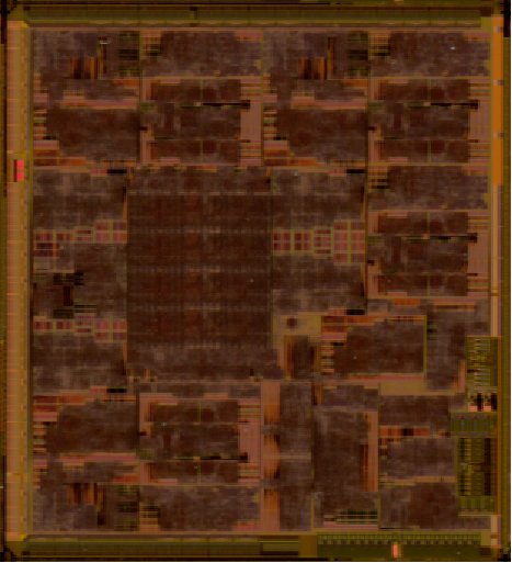
The 32MB of eDRAM is also the only thing presented that we can even draw a reasonable density measurement for. All of the rest is based on assumptions about what the blocks contain.
There are some ideas about some SRAM cell sizes on other parts of the die, like where Marcan thinks the ARM9 is. Maybe someone should look at what that density's like. Unfortunately I'm not aware that NEC has published SRAM density numbers nor am I aware of any other die shots with known quantities that we can compare against (this is assuming NEC manufactured, but at this point I think that's more likely - XBox 360 for instance used NEC to manufacture the eDRAM daughter dies)