Fourth Storm
Newcomer
I agree. But I must also say that the GPU and the layout of the SIMDs looks a bit strange. The size of the SIMD blocks would be consistent with a ~15% higher density layout than one sees in Brazos. Not completely impossible given the maturity of 40nm, AMD's experience with it, and the low clock target, especially if it uses an older iteration of the VLIW architecture (DX10.1 R700 generation instead of DX11 R800 generation) as base.
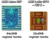
But there is more. I think function noticed already the halved number of register banks in the SIMDs compared to other implementations of the VLIW architecture. I glossed over that by saying than each one holds simply twice the amount of data (8kB instead of 4kB) and everything is fine. It's not like the SRAM stuff takes significantly less space on the WiiU die than it takes on Brazos (it's roughly in line with the assumed generally higher density).
But thinking about it, each VLIW group needs parallel access to a certain number (four) of individually addressed register banks each cycle. The easiest way to implement this is to use physically separate banks. That saves the hassle of implementing multiported SRAM (but is also the source of some register read port restrictions of the VLIW architectures). Anyway, if each visible SIMD block would be indeed 40 SPs (8 VLIW groups), there should be 32 register banks (as there are on Brazos as well as Llano and Trinity [btw., Trinity's layout of the register files of the half SIMD blocks looks really close to the register files of GCN's blocks containing two vALUs]). But there are only 16 (but obviously twice the size if we are going with the 15% increased density). So either they are dual ported (then the increased density over Brazos is even more amazing) or something really fishy is going on. Before the Chipworks guy said the GPU die is 40nm TSMC (they should be able to tell), I would have proposed to think again about that crazy sounding idea of a 55nm die (with then only 160SPs of course).
Thanks for the analysis. If the SRAM registers are dual ported, is this something that could be visibly discerned under close inspection?