Wii U hardware discussion and investigation *rename

Status
Not open for further replies.
In a pre-briefing interview with Hegalson before the press announcement went live, Gaming Blend had the opportunity to ask a few questions about the jump from mobile, PC and current-gen consoles to the first next-gen console, and whether developers would be able to make use of all of Unity's latest high-end technology on Nintendo's newest console, including the ability to make use of Unity 4's DirectX 11 equivalent features and shaders. Hegalson replied with the following...
Yeah. We'll do a -- we'll make it potentially possible to do.

What's interesting is that our philosophy is always this: We have a match work flow and I'm sure we can make a decent game and prototype, and they're fun. And then we have a shared system that basically allows you to access the full capabilities of the hardware you run. That's going to be good whether you're running [software] on an iPhone, the Wii U, a gaming PC or whatever.

When pried about the actual clock speeds, shader limits and memory bandwidth of the Wii U's GPGPU, Hegalson tried waving off the question, basically saying that it was up to Nintendo to disclose that information. Dang it.

http://www.cinemablend.com/games/Wi...ble-DirectX-11-Equivalent-Graphics-47126.html


Damn!
 
Grammar question : what's a match workflow? It can't mean were building games as if we were building cathedral and tower replicas with matches and glue.
 
Right now over at Gaf theres a huge debate over whats possible on the hardware front given the "WiiU's ~40w power draw". I really dont think that figure should be taken as a realistic average draw.

I doubt it, that's probably typical power consumption, imo. The power supply is rated a 75W and, imo it will probably be only 80% efficient or so, that will be probably around ~60W max at the WiiU. The WiiU has to be able to handle a degenerate case of the flash memory being accessed, all four USB ports being fully active, wifi and wireless controller link actives, disc drive spinning full speed, and CPU/GPU going all out, with probably some head room. That is unlikely, but possible. You can't have the Wii fail and potentially damage the unit in that case.
 
Regardless of the number of shader units, gflops, texture units, rops, etc., at least we know the console has 32MB embedded memory. This cannot be a bad thing :)
 
What is the consensus : SoC that integrates everything ruled out, or not?
CPU with eDRAM, paired with a GPU that communicates via a link?
Or even the to dies on an interposer, or packed in some way that allows both low cost and high bandwith.
Or ROPs migrated to the CPU die, if that makes sense.
 
Given the current power limits I would assume that an SoC is possible, the question is going to be was it practical given they were sourcing a "new" processor and a "new" GPU from two different vendors.
Integration for an SoC could be the reason they ended up with a DX10.X part from AMD, they may have had to lock the GPU design much earlier if IBM did the integration and manufacturing.
 
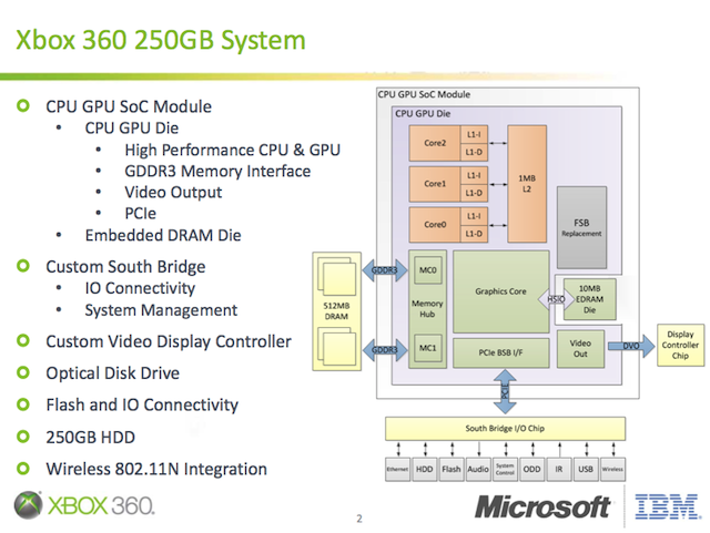
That makes a lot of sense, after remembering IBM made just such a chip when shrinking the xbox 360 to the same 45nm.
Basically repeating that job, with people that have gained the experience, just using more current designs was the easy and cheap thing. Here it is, an insta cheap console. That clears out the "why the hell is nintendo doing weird things again?" rage.

I also like to think this is the GPU tech AMD had in chipsets, so it was somewhat made to integrate with other components.
 
So for WiiU we are likely looking at a SoC design like the chip used in Xbox 360 Slim (?)


x360soc.png


I forgot the name of this chip and it isn't Valhalla since that name refers to the mb IIRC.

edit: I googled for a few minutes and found the name, it's called Vejle.
 
Last edited by a moderator:
So for WiiU we are likely looking at a SoC design like the chip used in Xbox 360 Slim (?)

Interesting, if the CPU and GPU are on one SOC. The GPU then had to be either shrunk from 55nm to 45nm or "grown" from 40nm to 45nm. Maybe that's why they supposedly started with a RV770 (55nm), since it's maybe easier to move down a half node instead of up.
 
IBM Watson
‏@IBMWatson
@Strider_BZ @BoostFire @Xbicio WiiU chip clarification: It's a "Power-based microprocessor" http://ibm.co/UhGspo

https://twitter.com/IBMWatson/status/248820933618442240


Interesting, if the CPU and GPU are on one SOC. The GPU then had to be either shrunk from 55nm to 45nm or "grown" from 40nm to 45nm. Maybe that's why they supposedly started with a RV770 (55nm), since it's maybe easier to move down a half node instead of up.
I hope this isnt the case. Gpu performance would take another nose drive. I hope they drop down to 32nm for the gpu.
 
It could possibly be a SoC assuming IBM is the one sourcing the edram for the GPU. Not sure of AMD's experience when it comes to making edram outside of Xenos, and I would think IBM offers a better solution anyway considering they've been using it for years now and kick ass with it.
 
I could be wrong but doesn't AMD have significant experience with edram because of the Flipper GPU in GameCube, the C1/Xenos GPU in X360 and the Hollywood GPU in Wii?
 
IBM is the best known maker of edram, using it as L3 two years ago (32MB and 45nm), and as L2 lately. AMD doesn't do it, the edram was, we can say, outside of Xenos.
That was 1T-SRAM I believe on nintendo GPUs, which is not quite the same thing.
 
IBM is the best known maker of edram, using it as L3 two years ago (32MB and 45nm), and as L2 lately. AMD doesn't do it, the edram was, we can say, outside of Xenos.
That was 1T-SRAM I believe on nintendo GPUs, which is not quite the same thing.

I don't quite understand.

Doesn't AMD have the collective experience of ArtX and ATI ?
 
To be pedantic :
- Their edram wasn't really dram. The tech used may have been lost, not suitable for a shrink or just abandoned.
- Even if you could make edram at a point, you have to develop working edram at each new process node and this is probably not trivial. Edram is not that widespread, we would maybe see them in microcontrollers if it were so. /edit : Well, a google search quickly tells me of a 16bit MC with 192K edram and a 32bit one with 1MB, so it's spreading a bit afterall :p
 
Last edited by a moderator:
I don't quite understand.

Doesn't AMD have the collective experience of ArtX and ATI ?


Sure they do, which pales in comparison to IBM's experience with edram. And 1T SRAM isn't the same as edram. It may be similar, but it's definitely not the same. One would hope IBM's edram tech is being used antd not AMD's.
 
Status
Not open for further replies.
Back
Top