Install the app
How to install the app on iOS
Follow along with the video below to see how to install our site as a web app on your home screen.
Note: This feature may not be available in some browsers.
You are using an out of date browser. It may not display this or other websites correctly.
You should upgrade or use an alternative browser.
You should upgrade or use an alternative browser.
The Intel Execution in [2023]
- Thread starter Wesker
- Start date
- Status
- Not open for further replies.
DegustatoR
Legend
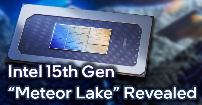
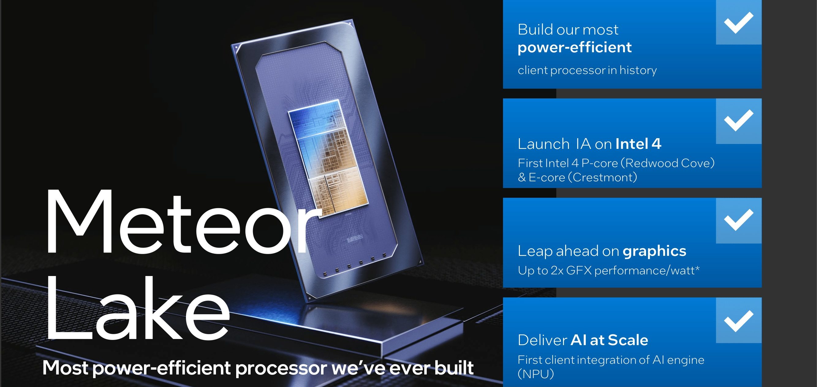
Meteor Lake details:
 www.techpowerup.com
 videocardz.com
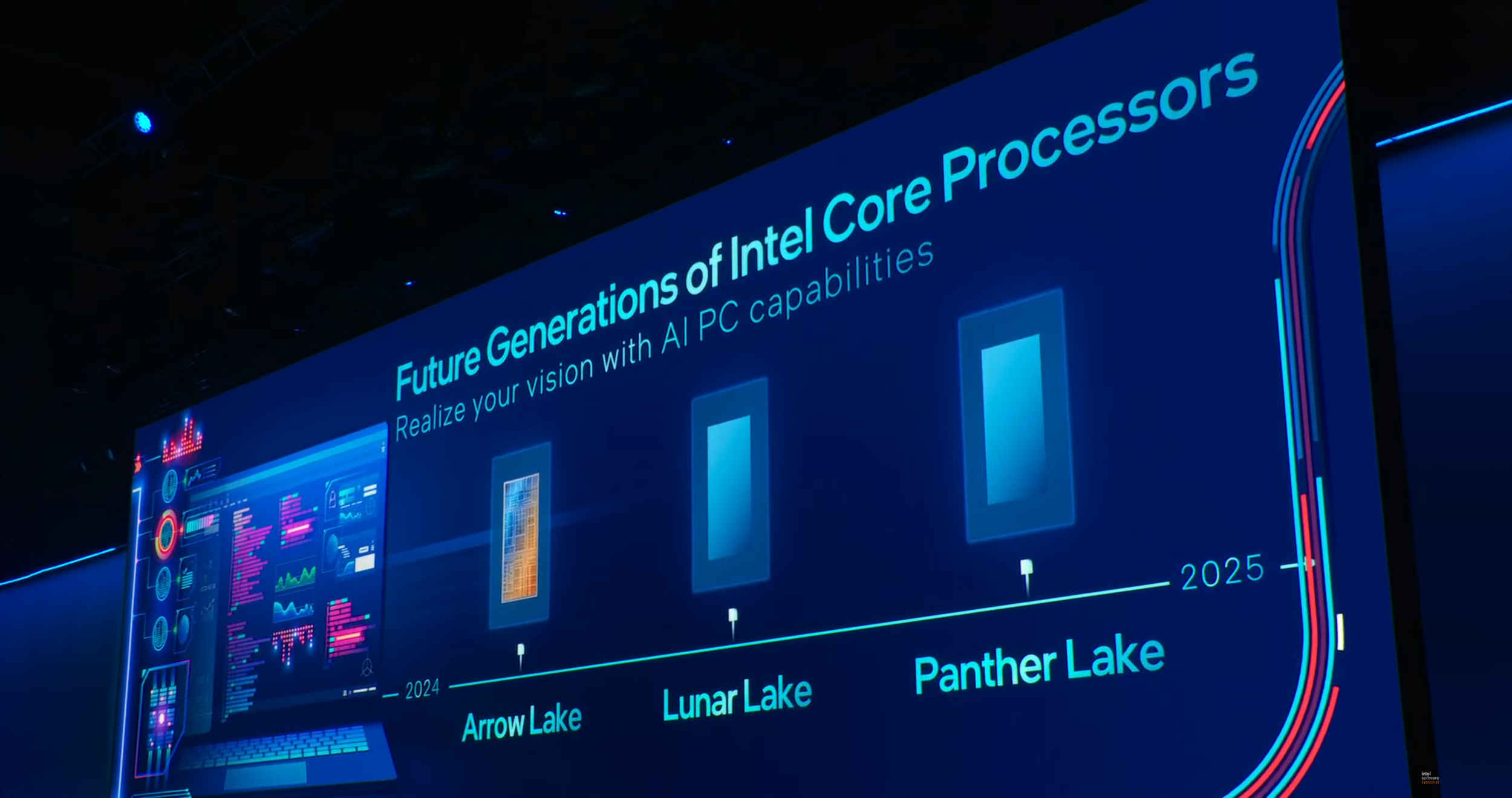
Future Intel CPUs:
 videocardz.com
Xe-LPG in MTL:

 videocardz.com

Intel Meteor Lake Technical Deep Dive
Today Intel is taking the wraps off their Meteor Lake Architecture. Our tech preview tells you everything you need to know about Intel's new ideas that will power the company's processors for years to come. Just like AMD, Intel is betting on chiplets, which combine multiple silicon dies into a...

Intel Core Ultra "Meteor Lake" CPUs officially launch on December 14th - VideoCardz.com
Intel announces Meteor Lake launch date, but no SKU information A detailed presentation on Intel’s next client CPU series “Meteor Lake” has been published right before Innovation 2023 opening keynote by Pat Gelsinger. Intel has revealed its next mobile Core processors, codenamed Meteor Lake...
Future Intel CPUs:

Intel confirms 2024-2025 client CPU lineup: Arrow Lake, Lunar Lake and Panther Lake - VideoCardz.com
Intel Panther Lake to enter labs in Q1 2024 The CPU maker has confirmed its next-gen client CPUs are on schedule. Intel has officially confirmed that the Meteor Lake (Intel 4 process) CPU series is set to hit the market on December 14th. However, Intel has an ambitious roadmap planned for...
Xe-LPG in MTL:

Intel details Arc "Xe-LPG" Meteor Lake GPU architecture, up to 8 Xe-Cores and ray tracing acceleration - VideoCardz.com
Intel Xe-LPG architecture delivers higher frequency and larger GPU configurations than Xe-LP A major upgrade to Intel’s integrated graphics. Meteor Lake GPU, Source: Intel Each successive iteration of Intel’s integrated graphics undergoes a 2x scaling enhancement, and the new Xe-LPG architecture...
So just to add onto this:I'm gonna use this soapbox to do a quick rant about why I hate Intel's chiplet approach:
They are gonna need SO MANY different dies. They are disaggregating so much, and clearly the intent is to try and have some sort of mix-and-match sort of thing going on, but this is never really gonna work, cuz of the constantly varying needs of every separate part. Not to mention that they're gonna need to have varying packaging sizes, including the critical and probably not cheap sort of base interposer(or whatever Intel is calling it) die anytime they want to provide some larger range of products.
And they're gonna struggle with this each and every generation. It would probably be less of an issue if most of these dies were being homegrown, but the fact that they have to produce so many on TSMC means very high design and manufacturing costs for each and every die.
Intel is racing ahead towards 'process leadership' like a lead footed drunk behind the wheel. Maybe they get where they're going, but in what shape will be they be when they get there? And it seems equally likely they crash somewhere along the way cuz they're betting the farm on everything working out, so I doubt they really have much in the way of contingency plans.
Just scares me. I know there's counter arguments for how this might well work out great, and I definitely want to believe so, but man.

This is:
3 x large base tiles
2 x GPU tiles(TSMC 5nm)
2 x SOC tiles(TSMC 6nm)
3 x CPU tiles
3 x I/O tiles
So all in all, that's 13 different tiles they need to produce to offer the scalability they want. And that's just for this series. Sure, some might be salvageable for later series, but it's still a LOT of different chips to have to produce/procure.
And it's just a whole lot of silicon as well. That 6P/8E version is really quite big as a whole.
Really dont like it. The simplicity of AMD's approach just seems so much better.
D
Deleted member 2197
Guest
It's what's possible, not what they'll do. Meteor Lake is currently 1 confirmed and couple rumored configurations, with GPU and IO tiles being the difference (the only confirmed configuration being the max config)So just to add onto this:
View attachment 9614
This is:
3 x large base tiles
2 x GPU tiles(TSMC 5nm)
2 x SOC tiles(TSMC 6nm)
3 x CPU tiles
3 x I/O tiles
So all in all, that's 13 different tiles they need to produce to offer the scalability they want. And that's just for this series. Sure, some might be salvageable for later series, but it's still a LOT of different chips to have to produce/procure.
And it's just a whole lot of silicon as well. That 6P/8E version is really quite big as a whole.
Really dont like it. The simplicity of AMD's approach just seems so much better.
edit: basedie doesn't need to change size even if the chips on top of it do, as long as it can accomodate the biggest configuration and you're not planning to fit the thing to a smaller package (which Intel has already confirmed they're not doing, with 1 package handling all the use cases instead of 3 of last gen)
Right, but the point is this is what they'd NEED to do in order to offer such scalability. Otherwise they're gonna be stuck with quite a limited number of offerings per series. This is their whole strategy going forward, not just with Meteor Lake.It's what's possible, not what they'll do. Meteor Lake is currently 1 confirmed and couple rumored configurations, with GPU and IO tiles being the difference (the only confirmed configuration being the max config)
edit: basedie doesn't need to change size even if the chips on top of it do, as long as it can accomodate the biggest configuration and you're not planning to fit the thing to a smaller package (which Intel has already confirmed they're not doing, with 1 package handling all the use cases instead of 3 of last gen)
You can be limited range per series, it's client stuff. Also you can scale by adding tiles, not just making them bigger.Right, but the point is this is what they'd NEED to do in order to offer such scalability. Otherwise they're gonna be stuck with quite a limited number of offerings per series. This is their whole strategy going forward, not just with Meteor Lake.
Btw I think I missed the context of why Intel decided to use TSMC for a bunch of stuff in meteor lake. Sure for the igpu, TSMC probably got better yield at the specs Intel wants. But for the other parts why also by TSMC?
Capacity issues on desired processes? They are all on modern processes after all.Btw I think I missed the context of why Intel decided to use TSMC for a bunch of stuff in meteor lake. Sure for the igpu, TSMC probably got better yield at the specs Intel wants. But for the other parts why also by TSMC?
You can be, but Intel tends to like offering large scalability with every series. Gonna be more difficult to do that now unless they just want to keep to manufacturing only the larger dies/packages and using cut down versions of those. At which point I'd just have to wonder what the point of going chiplet was to begin with.You can be limited range per series, it's client stuff.
Yea, there's little other reason when Intel 4 is a decent enough TSMC 5nm equivalent, and they of course also had Intel 7 to use instead of TSMC 6nm.Capacity issues on desired processes? They are all on modern processes after all.
But part of it could also probably just be contract agreements for TSMC. I dont think TSMC would have agreed to supply Intel, a fab competitor, with some short-term supply only, especially for more leading edge stuff. They probably had to commit to ordering a fairly high quantity of wafers.
Do they though? It's not that big range from 2 to 24 cores. You can use larger package and smaller dies too.You can be, but Intel tends to like offering large scalability with every series. Gonna be more difficult to do that now unless they just want to keep to manufacturing only the larger dies/packages and using cut down versions of those. At which point I'd just have to wonder what the point of going chiplet was to begin with.
Except when Intel has other stuff to fill all the Intel 4 & 7 capacity they haveYea, there's little other reason when Intel 4 is a decent enough TSMC 5nm equivalent, and they of course also had Intel 7 to use instead of TSMC 6nm.
I wonder if it wouldn't make sense to split the graphic stack in two, like what they did for compute.
Put the 2D part on the SOC so that it can be used for windows and only use the GPU for heavy duty applications like games.
In a way a 180 going back to the early days of separate 2D cards and 3D accelerators
Put the 2D part on the SOC so that it can be used for windows and only use the GPU for heavy duty applications like games.
In a way a 180 going back to the early days of separate 2D cards and 3D accelerators
DegustatoR
Legend
Windows is 3D since Vista though.I wonder if it wouldn't make sense to split the graphic stack in two, like what they did for compute.
Put the 2D part on the SOC so that it can be used for windows and only use the GPU for heavy duty applications like games.
In a way a 180 going back to the early days of separate 2D cards and 3D accelerators
I was agreeing with you on the last point, by the way. That was my point, too.Do they though? It's not that big range from 2 to 24 cores. You can use larger package and smaller dies too.
Except when Intel has other stuff to fill all the Intel 4 & 7 capacity they have
As for using smaller dies with a larger package, you can, but it still means having to produce more dies. And when they're doing GPU's and soon reportedly even CPU tiles on leading edge TSMC processes, this is gonna be expensive. It'd be different if they were doing everything with in-house fabs.
Yes, it could mean more dies, but realistically in client space you could do with 1 Compute (=CPU) tile as long as you can fit 2 of them in there for highend while lowend uses 1. Every Compute tile Intel has on it's current plans is on in-house processses up to Intel 18A (which if on schedule might actually tilt the scales on who has most advanced process online). Even going to just CPU cores themselves only ones not made in-house are LP-E's because they're part of SoC tile.I was agreeing with you on the last point, by the way. That was my point, too.
As for using smaller dies with a larger package, you can, but it still means having to produce more dies. And when they're doing GPU's and soon reportedly even CPU tiles on leading edge TSMC processes, this is gonna be expensive. It'd be different if they were doing everything with in-house fabs.
My curiosity is just how much money they'd actually save designing and fab'ing a whole new die rather than just using a 'cut down' larger one. Especially if they have to design and fab that die with an expensive TSMC process.Yes, it could mean more dies, but realistically in client space you could do with 1 Compute (=CPU) tile as long as you can fit 2 of them in there for highend while lowend uses 1. Every Compute tile Intel has on it's current plans is on in-house processses up to Intel 18A (which if on schedule might actually tilt the scales on who has most advanced process online). Even going to just CPU cores themselves only ones not made in-house are LP-E's because they're part of SoC tile.
I get your point, and you may be right. I just still think AMD has come up with a strategy that's just so much simpler that is still highly scalable. It feels like Intel is overcomplicating things in comparison.
oh well, I was used to seeing him in videos featuring Intel GPUs.... Wish him good luck wherever he goes. On a different note...
D
Deleted member 2197
Guest
Intel Arc A770 and A750 Content Creation Review (Sept. 2023 Update)
The Intel Arc Alchemist A770 and A750 launched 11 months ago. How have the Intel Arc A770 and A750 improved for content creation applications since then?
 www.pugetsystems.com
this affects all major GPU vendors.
 www.tomshardware.com

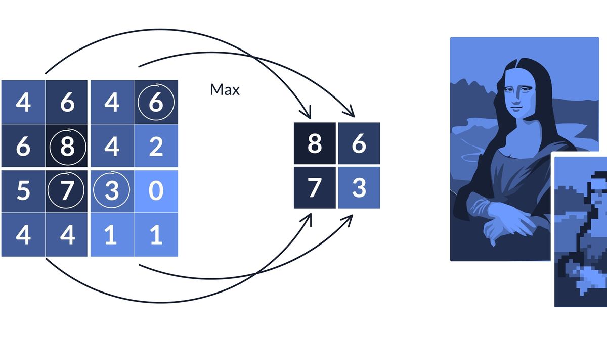
GPUs from Nvidia, AMD, Intel, and Others Vulnerable to Pixel-Stealing GPU-zip Attack
A side-channel vulnerability in GPU compression can reveal private details to malicious websites.
- Status
- Not open for further replies.
Similar threads
- Replies
- 3
- Views
- 2K


