R6xx Speculation - Implementation of Ring Bus for Multi chip interconnect.

Rishi

Newcomer
Hi Guys!

I have been a regular Beyond3D follower since nearly 4 years but this is the first time that i have thought of posting.

Especially with all the multi chip talk for the ATI r680 and r700.I thought it was high time a thread was started.

So heres what i think would be a nice idea, or may be some thing ATI already has up its sleeve in the RV670 ;).

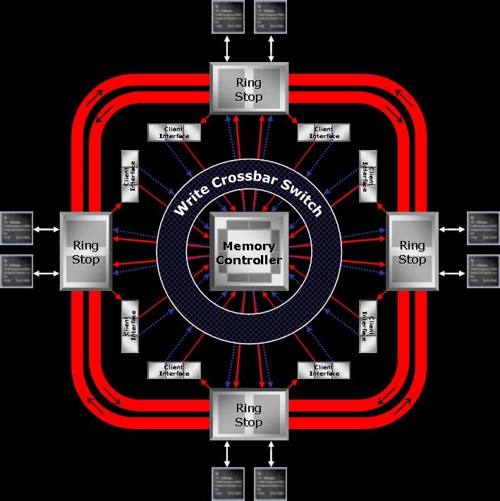
As we all know the R600 is a 1024 bit ring bus internally with 8x64 bit controllers and interfaces to a 512 bit external bus and the R520 had a 512 bit internal 8x32 organisation interfacing to a 256 bit external bus.

NOTE: In addition to these memory controllors there is an additional controller for PCI and video interfacing.

I am speculating that RV670 will have 4x64 bit controllers( 2 full duplex dual channel 64 bit memory controllers) in lieu of the 8x32 bit ones(4 full duplex dual channel 32bit memory controllers) and a Hypertransport interface for the controller sending requests to the ring stops on the bus.

This way with a sufficiently wide and fast hypertransport bus the multi chip module will have two RV670 die interfaced with a hypertransport interface and the package will have a 2x(2x64bit) controllers forming a 512 bit external interface.The ring bus width though could be the limitation, depending on a whether a bi directional 256bit or 512bit implementation is used.

The beauty of this design is that hypertransport interfaces easily with AMD processors for reusability for a multichip fusion design.

What do you guys think? Is it a viable design that can be expected in AMD designs or is it flawed?

I would really appreciate if you guys could point out flaws and present your ideas and opinions on multichip architectures for GPU's .
 
a Hypertransport interface for the controller
I think it's too soon for Hypertransport.

Rishi said:
present your ideas and opinions on multichip architectures for GPU's .
I'm not the most knowledgeable person (to put it mildly ;)), but I think that interconnecting physical chips to achieve better performance is viable idea only in > $390 market.
 
Nice thread.

I wouldn't be surprised if RV670 is 8x32-bit, rather than 4x-64-bit. Pictures of a board show the classic "asymmetric" memory chip layout that we associate with 32-bit connections.

A fundamental question with these MCMs is how tightly integrated will rendering be? Will all rendering be AFR based or will super tiling or scissored be usable? Even with AFR, are there opportunities to share memory equally for both chips, e.g. avoiding wasted RAM due to having textures copied to both memory pools?

Also, if the MCM has an effective 512-bit bus, is each chip going to be constrained by only having a 512-bit ring bus internally?

All this leads up to the question of the required bandwidth for the link between the two chips. 50GB/s? 100GB/s?

I like to reference the link we see between the mother and daughter dies for Xenos. That's 32GB/s.

Is Hypertransport the right kind of solution for more than 2 chips? I'm thinking we're likely to see a ring and mini-ring architecture on an MCM with the arrival of R7xx. A ring connecting the chips, with a ring inside each chip. I dunno if Hypertransport is amenable to a ring (is a ring a good idea for 4 chips?).

Though I also wonder whether R7xx's individual chips will have enough inside them to warrant an internal ring. A simple crossbar might be all that's needed (much like the crossbar between a shader unit, TUs and ROPs, connecting them all to a ring stop within R600).

Jawed
 
I think a picture speaks a thousand words .

I will try to modify one of the ring bus pictures from beyond3d to express my idea.

Hope the original owner doesnt mind.
 
53k9hn5.jpg


There guys ,i think this represents a more precise view of my earlier post .

I have combined the R600 diagram and R520 articles ring bus diagrams to better repersent my view.(Sorry i couldnt credit the person responsible for original pics.)
 
I was thinking a bit differently in that maybe one day we'd see the chips actually share the same ring bus as opposed to use a seperate bus like you drew. Maybe there would be a separate IO chip for display and PCI-E connections, or maybe it would just be part of each chip and disabled on all except one.

Worst case latency would increase with more chips, but scalability should still be better than SLI/Crossfire, and you wouldn't need to waste RAM by duplicating contents.

That sounds abit like the idea/drawing i had a few months back. Where basicly the ALU blocks are separate chips and connected through/with the ring-bus.

Edit: Dug up the link to that drawing. (excuse my rubbish mspaint skills) http://forum.beyond3d.com/showthread.php?p=1049128#post1049128
 
Last edited by a moderator:
I wonder if Hypertransport would be appropriate for an MCM bus.
If it isn't already there in the first place, there's no particular reason a lot of the specifications for HT should be implemented for a fixed MCM. If not Crossfire, there's a history of proprietary and slimmed-down bus connections, like SIS and its northbridge-southbridge connection.

If AMD wanted a Torrenza-type (maybe a HT expansion slot?) solution, but that might require a special chip revision all on its own and hurt any attempt by Fusion go above the low-end market.
 
I was thinking a bit differently in that maybe one day we'd see the chips actually share the same ring bus as opposed to use a seperate bus like you drew. Maybe there would be a separate IO chip for display and PCI-E connections, or maybe it would just be part of each chip and disabled on all except one.

Worst case latency would increase with more chips, but scalability should still be better than SLI/Crossfire, and you wouldn't need to waste RAM by duplicating contents.

Initially i had the same idea of using the Ring bus as the interconnect between chips, resulting in a big ring connecting the die on the MCM with unified memory access for all the die .This would eliminate duplicating content in the Graphics RAM and offer impressive scalability.

Thats when i realised that the Ring bus and the ring stops are being arbitrated at a central location.Thus the arbitration logic per chip should be capable of communicating with arbiters on the other chips to ensure coherency.
http://www.xbitlabs.com/articles/video/display/radeon-x1000_6.html

As you have said increase in the number of stops on the ring bus will result in a huge latency for accessing the memory and the width of the ring bus will have to be increased to accomodate for all the data that the ring stops can provide.

So a 4 chip MCM will require at least a 2048 bit ring bus.

That's why i felt that as the arbiters need to be connected for any MCM design why not connect them with a high speed Hypertransport Bus.

The Hypertransport bus can be used to gang the 2 chip solution as i have shown in my previous post or used to form a ring passing through in a 4 chip MCM.

More Hypertransport links could be added per chip for even higher scalability just like the Opteron's from AMD.The best thing is the possibility of adding AMD processors into the mix.

The only down side that i see is the increased arbiter complexity.Depending on how aggresive you are with the arbiter design , you could even desing the MCM to operate on a unified memory.
 
Thats when i realised that the Ring bus and the ring stops are being arbitrated at a central location.
AFA I remember, that's not the case for R600.

As you have said increase in the number of stops on the ring bus will result in a huge latency for accessing the memory ...
I doubt that the latency of the ring bus is in number of ring stops. It's more likely to be in the number of retiming pipe-line stages in between.
 
Thats when i realised that the Ring bus and the ring stops are being arbitrated at a central location.Thus the arbitration logic per chip should be capable of communicating with arbiters on the other chips to ensure coherency.
http://www.xbitlabs.com/articles/video/display/radeon-x1000_6.html
No, this is the key difference with R600, the memory system is fully distributed and it does things like cache snooping (or at least a patent describes it).

As you have said increase in the number of stops on the ring bus will result in a huge latency for accessing the memory and the width of the ring bus will have to be increased to accomodate for all the data that the ring stops can provide.

So a 4 chip MCM will require at least a 2048 bit ring bus.
I think it's reasonable to argue that on-MCM bus needs to be 2x the bandwidth of the off-MCM bus. I suspect 512-bits will be the limit for the off-MCM bus, simply because the pin count gets ridiculous.

I don't know how clock and width are constrained by an MCM (how many layers is cost effective for an MCM?).

More Hypertransport links could be added per chip for even higher scalability just like the Opteron's from AMD.The best thing is the possibility of adding AMD processors into the mix.
Fusion is potentially the best argument for Hypertransport.

Alternatively, what about using PCI Express 2.0 to connect chips? Each chip would have 2 16-lane PCIE ports.

Jawed
 
No, this is the key difference with R600, the memory system is fully distributed and it does things like cache snooping (or at least a patent describes it).

Jawed


Is the R600 ring bus substantially different from the R520, because the R520 has a central arbiter prioritising requests to the ring stops.

Just check this Quote from http://www.beyond3d.com/content/reviews/27/5

memring-big.jpg


As the diagram above illustrates the memory controller consists of the central controller, or arbiter, with the memory clients surrounding it that can make their data requests to the arbiter. All around the edges of the chip are two 256-bit ring busses, running at same speeds as the DRAM's, which run in opposite directions to reduce latency (dependant on where the data is going to or from it should only have to traverse a maximum of half the ring); by placing the memory bus around the edges of the chip wire density around the controller is decreased, which can result in higher clock speeds. There are 4 primary sequencer "Ring Stops" on the ring, where the data effectively gets on or off the bus, and on each of these ring stops are a pair of DRAM channels so that the ring bus is linked directly to the memory interface.

This is the flow of a client requesting some data (click the description for a pictorial representation):

A client makes a request to the arbiter.
The arbiter prioritises the request and, when ready, sends the request to a sequencer at the ring stop of the DRAM that houses the data.
The data is retrieved from the DRAM, then traverses the ring until it gets to the closest ring stop to the original requester client.

I have'nt found any papers, describing the Ring Bus in R600, to indicate the lack of central arbitration.

I would really appreciate if you could point me to one.
 
I think it's reasonable to argue that on-MCM bus needs to be 2x the bandwidth of the off-MCM bus. I suspect 512-bits will be the limit for the off-MCM bus, simply because the pin count gets ridiculous.

I don't know how clock and width are constrained by an MCM (how many layers is cost effective for an MCM?).
I agree with everything here. Obviously the BW of the interchip buses is the factor that decides whether this is possible or not. I assume they can be clocked much higher than the external bus, but width could be a big problem, especially if you want scaling to several chips where each chip has two neighbours. That's a lot of pads on the die.

Anyway, it's just dreaming for now. We'll see if ATI or NVidia go this route or not.
 
I agree with everything here. Obviously the BW of the interchip buses is the factor that decides whether this is possible or not. I assume they can be clocked much higher than the external bus, but width could be a big problem, especially if you want scaling to several chips where each chip has two neighbours. That's a lot of pads on the die.
I'm also assuming that an on-MCM bus can be clocked high.

Also, an on-die bus has an advantage over a memory-chip (off-die) bus: addressing and data lines are not needed, it's all multiplexed. This means less pads to implement the on-MCM connections than connections to memory. Power levels and noise problems should be less of a problem too. So I think connecting two or more chips together on an MCM should be notably less costly than it first appears, for a given bandwidth.

Jawed
 
That already happens in a limited fashion with current Crossfire. As for any MCM GPUs seeing the light of day, I think it's a given that AMD at least are looking at MCM parts for graphics, given statements earlier in the year (I think we covered some in our Develop '07 coverage).
 
I'd think the easiest implementation would be like with 7900GX2 but with the switch on package for an MCM & using faster PCIE 2.0.

Should be able to use the on die PCIE I/O ringstop without stuffing up ringbus latency.
The switch doesn't need to be only connecting two devices.
Being a switch, its only a matter of number of PCIE lanes supported by the switch to handle 4 or more devices.
 
Back
Top