"PS3 & Xbox360 in the Real World"

dskneo said:
I apologise to this forum, but this character as it coming for alooong time. The_game_master.


i understand why you talk like this in teamxbox.com, because nobody there understands things and you just have to join the words "Ps3... inefficient... no efective..." in the same post to have them look at you as a God because you say the things they say (x360 >ps3 no matter what) with technical talk, ergo, must be true for them.

The thing is, its beyond3d right here. That flawded talk doesn't pick fans here and i pitty those who keep staying in the dark with your talk at teamxbox. The positive things about some competition console, is no good to talk about, right? that means no respect over there.

With this guy, Every good thing on the little known Ps3 architecture is a Flaw compared to X360.
The only difference in your speach here is that you keep 360 out of the deal so nobody can suspect.
And then somebody with brains at teamxbox points out to this forum links to say otherwise, and you come up with a re-formulated 500 word essay (that you wrote hundreds of times already in there across endeless topics about the "good things in ps3"), on how about Rsx is inifficient and slow because its based on the G70 (which happens to be the Top gpu today), and you keep the trash talk how about it never will never hit 550mhz because you say so, even though its made at 90nm and that fact you never talk about.

After that Essay full with spectulation and omiting most of the good things, you go and talk Trash about this Article ( http://forum.teamxbox.com/showthread.php?t=364632 ) made by someone way better placed than you are at videogames, and you keep talking how the author must be crazy to talk stuff when RSX isn't even out yet...
....This being said, let me remind again about your 500 word essay of the same speculation (but way, way more negative) about how RSX is gonna suck with its huge limitations and never gonna reach 550mhz because Xenon is only 500 and that is no go for teamxbox, no sir. It must be Equal or worst than Ps3 by all means. 550 is impossible for rsx, but 500 is super doable in xenon, no doubt about it.
Oh, i forgot to mention that he says rsx is gonna be 420mhz FOR SURE, even though its a 90nm chip with all the advantages in thermaldinamics that it has.

I'm with high hopes that someone at teamxbox catches this post here... maybe you can start to give them things as they really are about the goods things of the opposition.

onde again, i apologize for this uncalled post. I'm new here, but i was cought in surprise when i saw this guy bringing his shortsight view about the other guys console in this respectable forum.

and yes, NUMA is a very very good solution to bring down the tipical bandwidth usage between Cpu and Gpu (such as a back buffer in a Gpu does) because in this case it keeps the cpu away from using bandwidth by not going to the Ram pool in the other side. It as his own memory to use without touching the main channel (so this one it can be free to transport the important stuff).
About the cpu and Gpu accessing/writing each others ram, no harm here. GPU couldn't care less about latency, and the GPu writting in cell ram i see no need for that.

You shouldn't feel the need to apologise for thegamemaster. Thanks for letting us know.
 
chachi said:
I think what's he's saying is it can't directly access the XDR but has to go through the EIB which is attached to the XDR memory controller.
Then he should say THAT instead of the other bunch of crap he wrote.

The RSX has to have some sort of memory interface to attach to the EIB
NO. RSX doesn't have ANY kind of "memory interface" attached to the EIB. It has a flexIO interface, which is like AGP, or PCIe in PCs, only much faster (from perspective of cell it's 2.5x faster read, 5x faster write compared to PCIe 16x.)

What you end up with is more latency than if you were going to the "native" memory pool
Well DUH, of course, but then keg decided to spice things up and attach a subjective opinion on the nature of the latency (calling it "terrible", or what was it?)

In reality it'll likely be in range of other off-chip memory accesses. Like I said, compare to athlon64 systems; do they suffer something awful in games? Doesn't mean it isn't an issue that has to be taken into consideration, but there's no need to put down the system by using subjective language like that. It's just fanb0yish sillyness.
 
Guden Oden said:
NO. RSX doesn't have ANY kind of "memory interface" attached to the EIB. It has a flexIO interface, which is like AGP, or PCIe in PCs, only much faster (from perspective of cell it's 2.5x faster read, 5x faster write compared to PCIe 16x.)
Po-tay-to, Po-tah-to. If you're using it to access the XDR memory pool then I'll call it a memory interface. :)

In reality it'll likely be in range of other off-chip memory accesses. Like I said, compare to athlon64 systems; do they suffer something awful in games? Doesn't mean it isn't an issue that has to be taken into consideration, but there's no need to put down the system by using subjective language like that. It's just fanb0yish sillyness.
IIRC the Athlon64 has the best memory latency of any modern processor due to it's on-die memory controller. It's already been stated here by developers who are likely to know that memory latency is going to be painful for both systems, it's going to be worse using XDR for the RSX but nothing you can't work around if the alternative is not having enough memory to do what you want to do.
 
chachi said:
Po-tay-to, Po-tah-to. If you're using it to access the XDR memory pool then I'll call it a memory interface. :)
No, you're not using it to access the XDR memory pool. You're using it to access the cell chip, which in turn accesses the XDR memory pool. It's an I/O port controller, and you can't call it a memory controller when it isn't. The on-chip GDDR dynamic memory controller functions completely differently to the packetized serial point-to-point interface of flexIO, the two aren't even remotely the same.

IIRC the Athlon64 has the best memory latency of any modern processor due to it's on-die memory controller.
But that is only for PROCESSOR memory accesses. Videocard memory accesses from the GPU have to go through AGP or PCIe to the AGP/PCIe-to-hypertransport tunnel chip (aka "northbridge"), then to the CPU's hypetransport controller, THEN to the on-chip DDR DRAM controller. Very similar setup to how RSX would access XDR memory in PS3, except the PC features much slower I/O and memory systems on every level.
 
Guden Oden said:
No, you're not using it to access the XDR memory pool. You're using it to access the cell chip, which in turn accesses the XDR memory pool.
What were we talking about again, the RSX accessing XDR for extra graphics memory, right? You can call it whatever you want but if you're using it for memory access at the time and touting it as a way to increase available graphics RAM then I'm not sure I see your point.

But that is only for PROCESSOR memory accesses. Videocard memory accesses from the GPU have to go through AGP or PCIe to the AGP/PCIe-to-hypertransport tunnel chip (aka "northbridge"), then to the CPU's hypetransport controller, THEN to the on-chip DDR DRAM controller. Very similar setup to how RSX would access XDR memory in PS3, except the PC features much slower I/O and memory systems on every level.
The point was regarding Cell's memory latency IIRC, something SMM had speculated about in his article. Why else bring up the Athlon64? :???:

About what you wrote, it kind of sounds like you're arguing Powderkeg's point for him here. The RSX <-> XDR pipeline would be much faster of course, but nobody uses AGP / PCIe texturing because it's too slow. Everytime the card would have to grab those textures the game would plotz. I don't think it'll be that bad, like I said before if the alternative is not having "enough" RAM then developers will work around any problems, but all things being equal they'd probably rather not have to do it.
 
Weren't you talking about Cell accessing GDDR3?
Which it can by the way, as it was specified by Sony that Cell can access video RAM (to mess around with the framebuffer for example) and RSX can access main memory (to get more textures if need be for example).
 
Wether it can or not wasn't even up for discussion, all Powderkeg and others were pointing out was that each chip has its own primary pool of memory and using the other will introduce some additional latency (compared to using its own pool).

Wether that additional latency has a terrible or negligible impact on performance is up in the air as far as we know. FlexIO was a much hyped feature for Sony so it certainly wasn't slapped in as an afterthought. It should offer more than enough performance for most intended tasks. No matter the cost though, in general it should be most desirable to stick with the chips local memory pool IMO...
 
Guden Oden said:
No, you're not using it to access the XDR memory pool. You're using it to access the cell chip, which in turn accesses the XDR memory pool. It's an I/O port controller, and you can't call it a memory controller when it isn't. The on-chip GDDR dynamic memory controller functions completely differently to the packetized serial point-to-point interface of flexIO, the two aren't even remotely the same.

Explain something to me, because apparently I'm wrong.

How does RSX know if it should access it's on-die cache, GDDR-3, or XDR memory to find a specific bit of data? I'm pretty sure a simple I/O port controller doesn't have that kind of logic.

And do you think the MMU might have something to do with it?


But that is only for PROCESSOR memory accesses. Videocard memory accesses from the GPU have to go through AGP or PCIe to the AGP/PCIe-to-hypertransport tunnel chip (aka "northbridge"), then to the CPU's hypetransport controller, THEN to the on-chip DDR DRAM controller. Very similar setup to how RSX would access XDR memory in PS3, except the PC features much slower I/O and memory systems on every level.

Then what's the point of having 32GB/sec GDDR-3 local video memory when the AGP bus only provides 2.1GB/sec bandwidth, and all memory access by the GPU has to run through that AGP bus?

What you are saying is that every video card since the GeForce 3 has the exact same memory bandwidth limitation, since they all are required to pass their data through a bus with the exact same bandwdith, regardless of what card you use.

Or perhaps the reason it's called "local video memory" is because it does not require going outside of the video card to access it.


What you are saying is correct for accessing the system ram, but it's not true for "video card memory" as you put it. And something is still telling the GPU which pool of memory it needs to access. Care to explain what that is?
 
Last edited by a moderator:
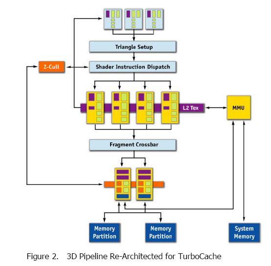
rsx.JPG
 
version said:


MMU = Memory management Unit


But I thought the RSX didn't have one of those. ;) And strange, according to that, the RSX does not use the FlexIO bus to access XDR.
 
Last edited by a moderator:
Keep in mind that Version loves to post tables and schematics of inexistant chips. Anyone remember his RSX-with-SPEs picture? :LOL:
 
london-boy said:
Keep in mind that Version loves to post tables and schematics of inexistant chips. Anyone remember his RSX-with-SPEs picture? :LOL:


Looks like he took a G70 block diagram, doubled everything and changed the ram from GDDR3 to XDR.
 
Wait, I'm confused... CELL <--> RSX takes place acorss the Flex I/O, right? So why is the XDR across the MMU? Wouldn't that seperate CELL from it's own pool of memory or are they orthogonal have completely seperate? Or am I just totally confused AND wrong, which I usually am.
 
Version, I'd love to have a link to the source of that diagram. In case you don't have one, I fear this page isn't an universally accepted source.
Sorry to reply to a potential trolling post by something else that could be considered trolling, but that diagram seems half-plausible if you don't think about it much. Problem is, it isn't, just like most other diagrams version posts; if this was true, it would imply:
- There are no VS units on the RSX.
- There are 8 quad pipelines and 16 ROPs.
- There is a MMU right in the middle of the pipeline, which I'm sure is a way to prove RSX can do memexport "better than Xenos".

Out of curiosity, how come this kind of posting is still accepted? Did version even ever get a warning for it in the past? Regarding the way RSX and XDR interact, Guden is right, at least based on the currently released information - since obviously there could be last-minute changes, but I very much doubt it.
Then what's the point of having 32GB/sec GDDR-3 local video memory when the AGP bus only provides 2.1GB/sec bandwidth, and all memory access by the GPU has to run through that AGP bus?
That's not what he said. That's what happens when the GPU tries to use SYSTEM memory; this can happen with certain usages of vertex buffers (highly suboptimal), or more importantly when using TurboCache. The GPU, of course, has its own GDDR memory controller for its onboard memory (which, in traditional PC architectures, the CPU *cannot* access directly or even half-efficiently).

As for the uses of the Cell writing directly to the RSX's GDDR3: Streaming, basically. This would let a good programmer get 99% efficiency with fully-streaming data compared to static data, should he waste enough memory for it (alternating frame principle because of syncrhonization issues).

Having the RSX access the XDR when streaming vertices would work too, and even more so considering it's not really a highly latency-sensitive part of the GPU pipeline and the bus is extremely fast. So that's an advantage, but not the biggest one. So, what's the biggest advantage? From my POV (and let me just remind you I don't program for consoles) it's not the writing to GDDR that truly matters: it's the reading.

If you look at how HDR is done for example, it could be done extremely well by a SPE. Heck, you could get more creative, and do a bunch of other things pretty fast that way; the problem though is that as others have said before, I wouldn't assume the SPEs to be well-tuned for FP16. Some speculated that's why NVIDIA talked of FP32 HDR, but I don't see where the memory footprint for that comes from; you could use lossy compression, but you'd need decompression to be extremely fast not only on the GPU, but also on the SPEs. Potentially less easy than it sounds.

If you just consider the "big bus" and the access to CPU/GPU memory through it for both components, you can't do much of anything better than if you only had a great CPU->GPU bus, or an unified memory system (ala XBox360). That doesn't make much sense however, considering the costs associated with that approach, so I'd personally expect NVIDIA to use a "few" transistors on the RSX for special functionality benefiting from this paradigm.

Uttar
P.S.: Yes, I wanted to finish on the word "paradigm". It just makes the whole thing look a lot less serious than it sounds, which is probably a good thing, since serious posts tend to generate flamewars, and "fun" posts tend to be spammy; combinations of both gotta be good thus - right?
 
Mefisutoferesu said:
Wait, I'm confused... CELL <--> RSX takes place acorss the Flex I/O, right? So why is the XDR across the MMU? Wouldn't that seperate CELL from it's own pool of memory or are they orthogonal have completely seperate? Or am I just totally confused AND wrong, which I usually am.

As i said, no need to get confused, version loves to confuse people with things that look real but actually aren't. I wouldn't worry about that RSX schematic too much.
 
london-boy said:
Keep in mind that Version loves to post tables and schematics of inexistant chips. Anyone remember his RSX-with-SPEs picture? :LOL:


That may be true, but this at least confirms the existence of a memory controller (memory management unit) in RSX, which some here seem to think it didn't have.


And wasn't it said earlier that there was a 500+ clock cycle delay in certain conditions? And I said that there was a 6 step memory access, with each step taking around 30ns minimum.

6 steps @ 30ns = 180ns.
Cell = 3.2 clock cycles per ns.

180 * 3.2 = 576 clock cycles.

I wasn't that far off, was I?
 
Powderkeg said:
That may be true, but this at least confirms the existence of a memory controller (memory management unit) in RSX, which some here seem to think it didn't have.

How does it confirm anything, as version made it himself :rolleyes:

Similar to your numerology involving the number 6...
 
Powderkeg said:
That may be true, but this at least confirms the existence of a memory controller (memory management unit) in RSX, which some here seem to think it didn't have.

Mmmmkay maybe the concept of MADE UP is hard to grasp.

Tha picture confirms nothing apart from Version's own dreams. RSX might or might not have a mem controller, but that fact certainly won't be confirmed by version's posts. Ever.

When we see schematics from Sony/NVIDIA, then we'll have confirmation.

(oh i love the little icons, i'm gonna try all of them from now on. Can we have more?)
 
Actually I expect RSX will have an MMU - since it's a key part of making TurboCache work.

This is because TurboCache is NVidia's name for the ability of the GPU to render into non-GPU memory (i.e. XDR in PS3) I think it's fair to say that RSX will have an MMU.

In theory G70 (7800GTX) has an MMU, because it supports TurboCache.

But the presence of TurboCache (MMU) doesn't imply a MEMEXPORT-like function. No, not at all
icon_smile.gif


Jawed
 
Back
Top