NVIDIA Tegra Architecture


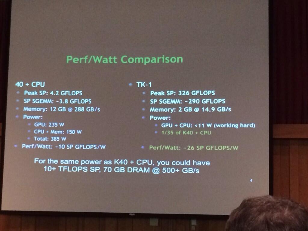
I don't think anyone sane ever believed that K1 has an as insane TDP as 60W. In any case the Tesla K40 vs. Tegra K1 slide has two distinct "errors"

1. The Tesla K40 obviously has a peak of 4.2 TFLOPs SP and not GFLOPs.
2. The Tesla system is compared on a TDP basis while Tegra K1 on a "SDP" basis (it states "working hard").

Here the slide in question:
Bl8_-GCCcAABW8r.jpg:large

https://twitter.com/ProfMatsuoka/media


The first link (softpedia? for crying out loud....) has the most technically entertaining title of them all:

NVIDIA TegraK1 SoC Finally Detailed, Has 5-8W TDP, 11W at TopLoad.
I don't think I'll bother to read an article where the author doesn't seem to have a clue what TDP stands for.

***edit: it would be nice for a change if all those wannabe authors like the bloke at wccf tech would actually have the courtesy to honor the actual sources where they get each bit from. Above is the link for the actual source and it's not like he was told by anyone else or that he has any actual sources, apart from constant plagiarism. The tweet in question is up there for around a week now.
 
I don't think anyone sane ever believed that K1 has an as insane TDP as 60W.
Well, one person at least thought that a 60W power adapter was a good enough indicator to write a hit piece. I thought that article was very useful for future usage, but probably not the way the author intended to be.
 
As a close second from the original 365 GFLOPs I saw recently 326 GFLOPs figures being mentioned and now it's suddenly just >300 GFLOPs. Either someone was just bored to calculate the 326 GFLOPs or not all Jetson K1 boards have the same GPU frequency.
Or in a multi-national company with thousands of employees, there are different people who write different texts with different emphasis?

As in: one marketing guy lists a maximum achievable performance number because they look good on a slide. Another one lists the maximum achievable specs of a particular implementation. Yet another one is a technical writer who doesn't particularly care because it highly depends on the application you're running anyway and he knows that his audience is smart enough to know that too.
 
Performance for those 32.5 fps in Manhattan offscreen was measured on the Jetson K1 board (which is not optimized for mobile power levels), yet the 7,29 fps/W were obtained from a mobile optimized platform. One result is not necessarily directly connected to the other.

Estimating TK1 perf. per watt on a mobile platform, and estimating AP+mem power consumption on different mobile form factors, will result in a reasonably good estimate of performance on said platforms.

At ~2.6w AP+mem power consumption (ie. equivalent to A7 in iPhone 5S), TK1 in an optimized mobile platform is ~1.45x faster than A7 and ~ 1.7x faster than S800. => ~19fps

At closer to ~4w AP+mem power consumption, TK1 in an optimized mobile platform should be ~2x faster than A7 and ~ 2.3x faster than S800. => ~26fps

At closer to ~5w AP+mem power consumption, TK1 in an optimized mobile platform should be ~2.5x faster than A7 and ~2.9x faster than S800. => ~32fps

The above estimate of 2.5x vs. A7 is coincidentally very close to the number NVIDIA showed on a chart a few months ago. Also note that NVIDIA is using iOS 7.1 results, so they are comparing to the latest and greatest drivers for that platform.

Note that, as impressive as Tegra K1 appears to be, Tegra M1 in Erista will be ~1.6x faster than Tegra K1 at all power consumption levels!

As a close second from the original 365 GFLOPs I saw recently 326 GFLOPs figures being mentioned and now it's suddenly just >300 GFLOPs. Either someone was just bored to calculate the 326 GFLOPs or not all Jetson K1 boards have the same GPU frequency.

There are various SKU's of Tegra K1, some which are lower performance than Jetson TK1 (presumably for smartphones and small, thin tablets), and some of which are higher performance than Jetson TK1 (presumably for micro game consoles that can make use of active cooling). Note that the 365 GFLOPS throughput number was really only mentioned in comparison to other consoles such as PS3 and Xbox360.
 
Last edited by a moderator:
I don't think anyone sane ever believed that K1 has an as insane TDP as 60W.

Then how about an insane 35-40 watts then: http://semiaccurate.com/2014/03/05/nvidias-tegra-k1-draws-shocking-number-watts

For the math averse, 5 * 12 = 60, so the power supply for this K1 demo is a 60W feed. If that number makes your jaw drop, you do get the right picture, this system has a massive draw. To be fair to Nvidia, the K1 demo almost assuredly does not pull anything near the 60W maximum for the power supply, it was warm to the touch but not blisteringly hot. In short it is pulling enough power to warrant its size but nowhere near the 60W max. Based on this and other information, SemiAccurate estimates a 35-40W draw for the entire system.
From this link: http://developer.download.nvidia.com/embedded/jetson/TK1/docs/Jetson_platform_brief_May2014.pdf

On page 13 you can see that the max board power is only 10.86 watts and the AP+DRAM is only 6.98 watts.
 
Last edited by a moderator:
On page 13 you can see that the max board power is only 10.86 watts and the SOC+DRAM is only 6.98 watts.

Oh that table quite specifically mentions "Platform power when delivering peak GFXbench3.0 Performance" and under "Power consumed at AC outlet" 12490 milliWatt. In simple english that means that Jetson is comsuming 12.49W while achieving those 32.5 fps in Manhattan offscreen; that's neither "max board power" in general nor TDP. My own estimate for at 2500/850MHz would be slightly below 20W TDP, but you'd have to find quite exotic corner cases to come as far to reach its TDP (as with practically the majority of platforms).

As for the rest you'd have to contact SA and its authors for further details.
 
Oh that table quite specifically mentions "Platform power when delivering peak GFXbench3.0 Performance" and under "Power consumed at AC outlet" 12490 milliWatt. In simple english that means that Jetson is comsuming 12.49W

Why are you using AC input power draw when the notes clearly state to use the DC power input:
8 AC power meters may have considerable measurement variances and it is recommended that power be measured at the DC power input of the board.
You are adding in 1.63 watts of the power brick AC-to-DC conversion to the board power when it has absolutely nothing to do with board power.

Also S|A used the DC side for power estimates not the AC side.
 
Even if I use DC results it doesn't change the fact one bit that any of the results are NOT equal to maximum power consumption or TDP. Anything substantial for that or do we have to waste more time over it?
 
On page 13 you can see that ... the AP+DRAM is only 6.98 watts.

Yup, and as mentioned earlier, the Jetson TK1 Dev. Kit is not optimized for mobile platforms, and as a result consumes ~ 40% more power than a similarly performing TK1 SKU that is optimized specifically for mobile platforms. So a ~ 326 GFLOPS GPU throughput variant of TK1 (operating at ~ 850MHz GPU clock operating frequency) optimized for a mobile platform would have AP+mem. power consumption of ~5w at max GFXBench 3.0 performance, which matches almost perfectly with the 5w TDP that NVIDIA specified for Tegra K1.
 
So a ~ 326 GFLOPS GPU throughput variant of TK1 (operating at ~ 850MHz GPU clock operating frequency) optimized for a mobile platform would have AP+mem. power consumption of ~5w with a GPU-heavy workload, which matches almost perfectly with the 5w TDP that NVIDIA specified for Tegra K1.

Excuse me but I just sprayed my soda all over the monitor ROTFLMAO :LOL:
 
You're entitled to your opinion and of course interepretation of anything that you read. But that's about it.

NV for the record nowhere used the description "TDP" wherever they stated 5W, so you may spend the rest of the evening looking for it while I clean up this mess here.
 
Even if I use DC results it doesn't change the fact one bit that any of the results are NOT equal to maximum power consumption or TDP.

That may be your belief but without any published facts showing otherwise I will use the actual published data for the Jetson TK1 Development Platform Power for reference.

I also look forward to see results (performance, power) from those who have actually purchased the Jetson TK1 Development Platform.
 
Last edited by a moderator:
There's no TDP published for Jetson or any K1 and NVIDIA doesn't actually need to because it's not something that usually appears in the ULP mobile world.

That is of course if you actually understand what TDP is actually referred to. A GTX770 desktop GPU for example has a TDP of 230W irrelevant if it's typical peak power consumption in games/applications is usually in the 160-170W ballpark. You're looking for the latter comparable measure for K1 not the first.

Last but not least Manhattan in Gfxbench3.0 is quite GPU ALU bound; it doesn't mean that the CPU cores are sitting around idling, but it doesn't mean either that you've put the maximum possible workload on them either.
 
This is just semantics. At the end of the day, the TK1 application processor + mem. in a mobile platform will consume up to ~ 5w (sometimes a bit less, sometimes a bit more) with very processor-intensive applications using this SKU. Obviously the power consumed will be allocated based on CPU/GPU workloads, but total power consumed by AP+mem. will likely almost never be significantly higher than 5w due to form factor constraints in the ultra mobile space. And FWIW, NVIDIA did specifically state on slides that Tegra 4 has a "5w TDP", so I see no reason to believe that Tegra K1 will be any more power hungry when used in the same or similar form factors.
 
NVIDIA as many other SoC manufacturers don't address just one market and there are obviously differences between different markets. Tegra4 has Shield which is actively cooled and no the TDP for the entire SoC at peak frequencies isn't anywhere near 5W TDP, as the A7 in iPadAir isn't either and many other high end SoCs out there. Guess what they're all above that metric and it's not a sin either.

That slide a couple of posts above is the laughing stock of the past decade. If you'd compare a high end system with a K40 against a Tegra K1 on a true apples to apples basis the latter might come out with a more favourable ratio but nowhere the difference they're showing. It's not like they're all of the sudden are designing "junk" for the high end and Tegra is the new found wonderpuppy against it. IMHO the difference between the two could be around 50-60% in favour of K1 for SGEMM SP FLOPs but nowhere near the 160% difference they're trying to show.

In summary yes it's true that ULP mobile SoC GPUs have a surprisingly high SP GFLOP/W ratio, but that's about it then, since all "miracles" will always be bound to N SoC bandwidth at any time shared by all different SoC units and not just dedicated high bandwidth rates for the GPU. That's just how much "semantics" really are; oh and yes marketing stinks everywhere it's just how naiv anyone is to believe everything blindly and that goes for any IHV out there.
 
The thing I don't like about all this talk about power consumption under heavy load is that we have no good idea what the perf/W curve of the CPU cores is actually like in this scenario. I don't have the first idea what the CPU load is like on GFXBench 3, I just know it's heavily GPU limited on all mobile SoCs, so probably not a huge CPU load. Saying that GFXBench 3 is a good indicator of peak load may not be accurate; it may not even be a good indicator of what a GPU intensive game will use. It also makes the comparison with the Tesla system that much more inappropriate (where they include the entire TDP of the CPU used!)

nVidia had a good slide showing a perf/W curve for the CPU cores, now I'd like to see some real world measured data to back those claims up. It's too bad we can't get instrumented power numbers for the GPU and CPU rails separately, and tested under both real world GPU and CPU intensive applications.
 
AOC's All-in-Ones

Using older T3 SOC but in a 22" for only $299.

http://techreport.com/news/26415/aoc-android-powered-all-in-one-systems-start-at-300

AOC has uncorked a couple of affordable all-in-one systems that run the mobile OS. The machines have all the touchscreen goodness one might expect from Android-based devices, plus enough USB ports to connect a keyboard and mouse. They also sport HDMI inputs, allowing signals from other systems to be fed to the display.

...

Both machines use a quad-core Nvidia T33 SoC from the Tegra 3 generation. They have 2GB of RAM and are limited to just 8GB of flash storage.

Fortunately, the onboard flash can be expanded via an SD card slot. The four USB 2.0 ports provide plenty of options for secondary storage, too. Additional devices can be connected via Bluetooth. You also get a 720p webcam and 802.11n Wi-Fi support.

Users can choose between 22" and 24" models, both of which employ IPS panels with 1080p display resolutions. The 22" version is set to sell for $299.99, while its 24" sibling is priced at $399.99.
 
Back
Top