NVIDIA Tegra Architecture

http://images.anandtech.com/doci/7905/Jetson_Pro.jpg

That's the Jetson Pro pic in Anand's article; the other two pictures in that writeup are both from Jetson K1 one without a fansink and one with one.
If people are talking about a Jetson with big heatsinks, this may be the image they've seen:

http://www.nvidia.com/content/tegra/automotive/images/jetson/jetson-0063-0068.jpg

That's a side shot of a Jetson Pro configuration. The lower boards are the EBBs and the T3 board is the top board, as close as I can tell.
 
5rozt.jpg


Jetson K1 with big heatsink on the Tegra module, and a fan. That's the automotive one I alluded to.
 
Yeah, and the module is swappable (and the K1 module clearly uses a heatsink). My point here is that there are K1s with heatsinks and fans, and there are some without (new Jetson).
 
If Jetson Pro with a Tegra 3 has a bigger heatsink than Jetson TK1 with a Tegra K1, then the only obvious conclusion here is that Tegra 3 can't possibly fit inside a phone or tablet.

Right?
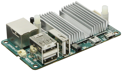
Heh. I'm afraid people don't realize many existing phone/tablet SoC need a heatsink if they are run at full speed all the time, which is how some devs use their devboards.

Here is an example with Cortex-A9 based Samsung 4412:
http://hardkernel.com/main/products/prdt_info.php?g_code=G138733896281&tab_idx=1
201312222305368236.jpg
 
Exactly. I'm delighted to see that the discussion here hasn't descended to a level where the size of the power brick is used as an indicator of the power consumption under typical load (yes, some people are *that* stupid), but the presence or the size of a heatsink alone isn't that much better.

The reality is that you need cooling the moment you go above just a handful of Watts. And if you reduce the problem space to just the die size, the process, and the clock speed at which as certain precent of the logic on that die is running, you will end up with 10W+ on pretty much all of the latest and greatest SOCs in worst case full load.

The competitiveness of mobile SOCs is a matter of tens of percent more or less for a particular workload. That kind of variance is not an amount that would determine whether or not you need a beefy cooler under such worst case full load.

Which means that the need for such cooler in a dev kit is an indicator of absolutely nothing.

In other words, as long as we don't see numbers of an SOC tuned to an actual product, there's very little to discuss. (Yes, that's boring.) But I'm under no illusion that this will stop the power brick analysts or those who think a difference of 40M flops between a marketing slide and an actual dev kit is a smoking gun.
 
That's the thing. You can see per-SoC configs of K1 limiting clock for the kits without fans. These kits are used for form-factor development. So you expect that the kit will somewhat accurately represent what's possible in a form factor device, performance and power wise, including long-term operation.

Nobody is saying all K1s need a fan. But clearly some will at certain performance levels. There's nothing wrong with that either, fans aren't taboo in embedded land.
 
I have a fan blowing at me right here at the office at work (until they fix the damn air con). Either way chicks consider me a "hot" guy.... in a very metaphorical far fetched sense :LOL:
 
Old jetson was used for the development of the in-vehicle system with the thing which combined gk208 with tegra3

I think that it is really stupid to make noise to see this old type
 
I think that it is really stupid to make noise to see this old type

No one is making any noise; the last few pages were merely about expectations. If you have a table where NVIDIA actually clearly states for which target market they're going to clock the GK20A at a specific frequency feel free to show it to me. All they have done is to show the maximum frequency of the design.
 
http://www.digitimes.com/news/a20140328PD213.html

Taiwan Semiconductor Manufacturing Company (TSMC) is likely to add two more advanced processes to its 16nm process portfolio in order to compete with the 14nm nodes to be released by Intel and Samsung Electronics, according to industry sources.

According to TSMC's original roadmap, the 16nm FinFET process is expected to enter trial production at the end of 2014. But TSMC now plans to release a 16nm FinFET+ process also at the end of 2014 and a more advanced 16nm FinFETprocess in 2015-2016, the sources noted.

The 16nm FinFET+ process is expected to enter volume production in early 2015 and may help TSMC win A9 processor orders from Apple, the sources indicated.

Some mobile fabless customers may directly adopt the 16nm FinFET+ process since it gives an additional die shrink, while migrating from 20nm, according to JP Morgan Securities.

The more advanced 16nm process is tentatively named as 16nm FinFET Turbo, the sources noted.
 
Digitimes pffff............:rolleyes: In any case if there's any merit to the sentence in the middle it's anything but good news for anyone else manufacturing at TSMC.
 
What does this have to do with the Tegra roadmap exactly?
Digitimes pffff............:rolleyes:
Whats wrong with Digitimes? I know they aren't the best..but they're right more often than not.

Either ways..this is old news already and was announced back on Feb 20th - http://community.arm.com/groups/soc...-finfet-and-arm-s-64-bit-biglittle-processors
In any case if there's any merit to the sentence in the middle it's anything but good news for anyone else manufacturing at TSMC.
If you're referring to the bit about Apple..it seems like just speculation again. We've been hearing about Apple moving orders to TSMC since the early days of 28nm and so far we've seen nothing.

Unless they are willing to hike capex substantially, I do not think TSMC has enough volume on the leading edge processes to cater to Apple. Not unless they're willing to piss off all their other customers and I'm sure they don't want to do that. If you look at 28nm for example, IIRC TSMC 28nm was pretty much at full capacity through 2011-2012 and did not really have any spare capacity till 2013.


Anyway coming back to things Tegra related..any news on Erista? Will it be like Tegra K1 with a quad Cortex A57 (possibly BIG.Little with A53) and a separate Denver based SoC? Or will they move to just one SoC with Denver cores.

GPU of course is expected to be something like GM208 and the timing suggests its on 20nm. I haven't received any info on tapeout. Will try finding out.
 
Whats wrong with Digitimes? I know they aren't the best..but they're right more often than not.

Since you know that their track record isn't exactly admirable, why are you asking in the first place? :LOL:

If you're referring to the bit about Apple..it seems like just speculation again. We've been hearing about Apple moving orders to TSMC since the early days of 28nm and so far we've seen nothing.

Well they are for 20SoC as it seems and while I've no idea if they'll also use Samsung to dual source rumors so far say no but you can't trust them either. Who said they'd manufacturing on 28nm/TSMC?

Unless they are willing to hike capex substantially, I do not think TSMC has enough volume on the leading edge processes to cater to Apple. Not unless they're willing to piss off all their other customers and I'm sure they don't want to do that. If you look at 28nm for example, IIRC TSMC 28nm was pretty much at full capacity through 2011-2012 and did not really have any spare capacity till 2013.

And I don't think that Apple intends to use TSMC ever as single source; in fact I rather think that 20SoC for A8 is just a singled out case. But I can however believe that TSMC would still want a piece of their future manufacturing case and hence my question where the good news exactly are. If it turns out to be true it's only good news for TSMC and Apple.


Anyway coming back to things Tegra related..any news on Erista? Will it be like Tegra K1 with a quad Cortex A57 (possibly BIG.Little with A53) and a separate Denver based SoC? Or will they move to just one SoC with Denver cores.

No idea but I consider it absurd to have both A57 cores and Denver SoCs. For K1 they probably created a second variant with Denver to jump asap on the 64bit train.

GPU of course is expected to be something like GM208 and the timing suggests its on 20nm. I haven't received any info on tapeout. Will try finding out.

2 SMMs sounds reasonable.
 
Anyway coming back to things Tegra related..any news on Erista? Will it be like Tegra K1 with a quad Cortex A57 (possibly BIG.Little with A53) and a separate Denver based SoC? Or will they move to just one SoC with Denver cores.

GPU of course is expected to be something like GM208 and the timing suggests its on 20nm. I haven't received any info on tapeout. Will try finding out.

According to NVIDIA's CEO, Erista is "right around the corner". I take that to mean that first silicon for Erista will be back from the fab. within ~ 3 months (with mass production starting ~ 9 months after that).

As for choice of CPU cores, I would think that NVIDIA needs to stick with it's guns and use fully custom Denver cores moving forward, rather than a mix and match approach. It would be strange to spend the last 5-7 years working on a fully custom Denver CPU, use it in Logan v2, and then abandon it in Erista v1. Each new generation of Tegra should always be more advanced and more sophisticated than the prior generation in all areas.
 
According to a Chinese news site, Microsoft will be unveiling an 8" Surface Mini powered by Tegra K1 on April 2.
 
It's not that great a market for Tegra, as a Surface is locked down and can only run Metro apps ; its competition is Atom tablets that can run everything.
You have to be o.k. with the hardware being locked down like an iphone. That stuff isn't tolerated on x86. Why can't I run desktop linux if I want to, given that the chipset supports it.

There will probably be the same tablet or almost in an Android version, less locked down. Or wait for the Surface K1 to get hacked.
 
No idea but I consider it absurd to have both A57 cores and Denver SoCs. For K1 they probably created a second variant with Denver to jump asap on the 64bit train.


2 SMMs sounds reasonable.

I agree it doesn't make sense, but a less absurd option is to have A53 cores (and only them).
A 3rd party SoC vendor would license the nvidia GPU tech and build the lower end SoC, not nvidia.
Cortex A12 is another option (32 bit)

I think we've not heard anything since the announcement last year that nvidia was open to licensing its GPUs?
 
Back
Top